Surging Number of Applications to Drive Semiconductor Metrology and Inspection Market during 2022–2028
According to our latest market study on "Semiconductor Metrology and Inspection Market Forecast to 2028 – COVID-19 Impact and Global Analysis – by Type, Technology, and Organization Size," the market is expected to grow from US$ 7,553.00 million in 2022 to US$ 8,288.55 million by 2028; it is anticipated to grow at a CAGR of 6.6% from 2022 to 2028.
Semiconductors are used in many digital consumer items, including mobile phones/smartphones, digital cameras, televisions, washing machines, refrigerators, and LED bulbs. Recent advancements in semiconductor chips offer automation in lighting in smart buildings. Lighting systems with semiconductor chips embedded within the luminaries allow sensors to draw on the same energy source as the lights in today's smart buildings to manage light autonomously. These sensors can measure the amount of light necessary in real-time and relay that information back to the management system. Also, Industry 4.0 is augmenting the usage of semiconductors for industrial sector. These factors contribute towards semiconductor metrology and inspection market growth.
The number of semiconductor devices put in automobiles has been continually increasing. Car-mounted semiconductors are available in a variety of shapes and sizes. More semiconductors are likely to be employed in Advanced Driver Assistance Systems (ADAS) in the future. Thus, the growing demand for semiconductor-based products bolsters the semiconductor metrology and inspection market growth.
The APAC semiconductor metrology and inspection market is segmented into Australia, India, China, Japan, and South Korea. The growing adoption of smart electronic devices is boosting manufacturing possibilities. One of the primary forces driving the market in the region is the increased incorporation of electronics in automotive applications. In addition, the integration of IoT (Internet of Things), AI (Artificial Intelligence), and connected devices across multiple end-use verticals is likely to drive the semiconductor metrology and inspection market during the forecast period.
As per our semiconductor metrology and inspection market study, the ecosystem comprises of following stakeholders- hardware/component providers, semiconductor metrology and inspection manufacturers, metrology and inspection service providers, and end-users. The component providers offer various components such as lenses, switches, motors etc. Often R&D partners of metrology equipment providers also become component providers. The semiconductor metrology and inspection market players such as KLA Corporation, ASML and Applied Materials provides the equipment to metrology and inspection service providers or directly to the end user, such as Taiwan Semiconductor Manufacturing Company, Intel Corporation and Samsung Corporation.
The semiconductor metrology and inspection market is segmented on the basis of type, technology, and organization size. Based on type, the market is segmented into wafer inspection system, mask inspection system, thin film metrology, bump inspection, package inspection, lead frame inspection, and probe card inspection. By technology, the semiconductor metrology and inspection market is bifurcated into optical and e-beam. Based on organization size, the market is bifurcated into large enterprises and SMEs. The large enterprises segment led the semiconductor metrology and inspection market share in 2021.
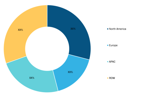
Semiconductor Metrology and Inspection Market Share — by Geography, 2020
Semiconductor Metrology and Inspection Market Analysis by Size & Share 2028
Download Free SampleSemiconductor Metrology and Inspection Market Forecast to 2028 - Analysis By Type (Wafer Inspection System, Mask Inspection System, Thin Film Metrology, Bump Inspection, Package Inspection, Lead Frame Inspection, and Probe Card Inspection), Technology (Optical and E-Beam), and Organization Size (Large Enterprises and SMEs)
Applied Materials, Inc.; ASML; Hitachi High-Tech Corporation; JEOL Ltd; KLA Corporation; Nova Ltd.; Nikon Metrology NV; Onto Innovation; Thermo Fischer Scientific Inc.; and Lasertec Corporation are among the key players profiled during this study on the semiconductor metrology and inspection market study. In addition, several other important market players were studied and analyzed during this market study to get a holistic view of the global market and its ecosystem.
As per the Organization for Economic Co-operation and Development (OECD), the COVID-19 pandemic affected major countries such as India, China, Australia, and Japan, which also experienced inflation. Several economies in Asia Pacific experienced a sharp decline in their GDP in 2020 due to the sudden closedown of the majority of economic activities across the region. India was the worst-hit country by the pandemic in the region. The limitations imposed by governments to control the spread of novel coronavirus during the initial time of the outbreak in the mentioned countries affected the production process due to the restriction of the limited workforce. Automotive and consumer electronics are key sectors that contribute to the growth of the semiconductor metrology and inspection market in the region.
The region's largest semiconductor producers, including Japan, Taiwan, and South Korea, witnessed some losses due to the restrictions on the supply chain in 2020 as these countries export their semiconductors to several countries. However, as the economies reopened and industries resumed their operations, the demand for semiconductors from various end users has started to grow gradually.
Contact Us
Phone: +1-646-491-9876
Email Id: sales@theinsightpartners.com