
Photomask Market Key Companies and SWOT Analysis by 2027
Historic Data: 2016-2017 | Base Year: 2018 | Forecast Period: 2019-2027
- Status : Published
- Report Code : TIPAR100000388
- Category : Electronics and Semiconductor
- No. of Pages : 151
- Available Report Formats :


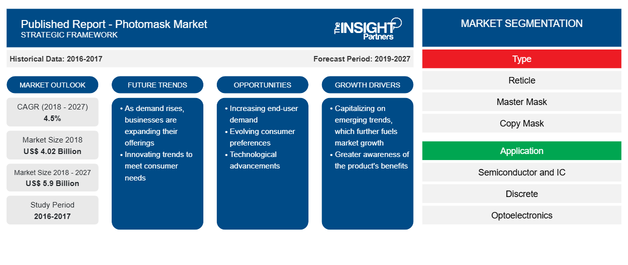
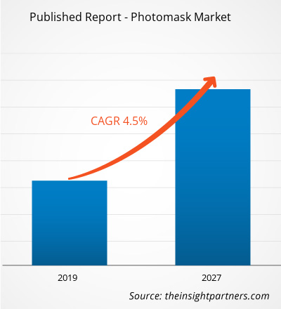
The photomask market was valued at US$ 4.02 billion in 2018 and is projected to reach US$ 5.9 billion by 2027; it is expected to grow at a CAGR of 4.5% during 2019-2027.
Photomasking is a process used in the microlithography process for manufacturing of Integrated Circuits (ICs), Micro Electro Mechanical devices (MEMS), semiconductors, PCB and photonic devices. Popularly the photomask is called as the master copy for patterning as it acts like a negative film in photography. With the process of photolithography, photomasks transfer the pattern onto the baseplates of circuit boards. The design in a photomask consists of binary pattern that replicates the original design which needs to be imprinted on the baseplate or the circuit board. The binary pattern on the photomask modulates the intensity of light in the lithography process to print the design on the substrate or the silicon wafer being used. The photomask itself is made using a glass substrate or fused silica that is coated with an opaque film.
The short lifecycles of electronic devices, high memory requirements in small storage memory chip sizes are a few factors that are bolstering the market growth for photomasks well as the increasing adoption of those tools in semiconductor manufacturing industries, particularly in developing economies, resulting increase in demand for photomasks. Many companies such as Nippon Filcon Co Ltd., Taiwan Mask Corporation, Hoya Group, Photronics Inc., Toppan photomasks among others are investing in photomask owing to the potential improvements related to accuracy, operational efficiency and timely order fulfilment thereby, helping them to enhance customer retention rate and compete efficiently in the market.
Factors such as the shift in display of mobile devices from LCD to LED and AMOLED along with penetration of IoT concept is increasing the demand for FPD (Flat Panel Display) along with IC photomask as new design requires a new set of photomask. Additionally application of MEMS systems (Microelectromechanical) in the automotive, consumer electronic and Bio-MEMS industry is also going to generate a strong demand pull for newer set of photomask. Increasing mask complexity is also going to drive more mask layers per set tighter geometries on each layer in the photomask market.
Customize This Report To Suit Your Requirement
Get FREE CUSTOMIZATIONPublished Report - Photomask Market: Strategic Insights
-
Get Top Key Market Trends of this report.This FREE sample will include data analysis, ranging from market trends to estimates and forecasts.
Market Insights–Photomask Market
Growth of Manufacturing Sector Using Semiconductor Devices in Asia Pacific
Abundant manpower resource and natural resources make Asia Pacific as one of the most ideal places for setting up manufacturing plants. Being a region dominated by developing countries, technological advancements in Asia Pacific are gradually taking pace with the help of western influence. As a result, the manufacturing plants are seeking for a paradigm shift from traditional methods of operations to achieve better cost and operational efficiencies. The manufacturing sector for consumer electronics, automobiles, textiles, consumer goods etc. are the largest contributors towards the flourish of the sector.
Incorporation of automation in the manufacturing sector is possible only with the help of high power semiconductors and IC chips. In a bid to meet the global demands, the production capacity of the manufacturing plants need to be stepped up and the number of semiconductor devices incorporated in the machines will also increase parallel to this. Moreover, Governments in China, India, Japan and Singapore have been supporting in-house manufacturing with programs such as “Make-in-India”. Programs of these kinds ensure huge influx of investments into the economy. Investments enable adoption of high-end technologies.
Photomask tools for ensuring the availability of these semiconductors and ICs will also be highly in demand and the market for photomasks would thus be driven with booming manufacturing sector of Asia Pacific.
Type Segment Insights
Based on type, the photomask market is segmented into reticle, master mask and copy mask. Different type of photomasks plays a major role in providing assistance for the production ICs and other semiconductor chips. Also, for the mass production of TFT array and color filter of TFT-LCD panels, the photolithography technology transfer photomask graphics onto the base material of the LCD panels.
Application Segment Insights
Based on application, the photomask market is bifurcated into semiconductor and ic, discrete, optoelectronics, display device, mems, and others. Photomasks find their largest applications in the manufacture of semiconductors. A set of photomasks is required to produce a complete semiconductor material. The photomask is protected by in this case is protected by a foil which is called pellicle to avoid any contamination to the chip board. The image carved on the photomask is then imprinted on the chip board by laser lithography or e-beam lithography.
End User Vertical Segment Insights
Based on application, the photomask market is bifurcated into semiconductor & IC and flat panel display. Photomasks find their largest applications in the manufacture of semiconductors. As per Ohio research, nearly 90% of all household devices are manufactured through silicon wafers, whereas 30% of different toys and 45% of industrial machines are developed and manufactured by incorporating silicon wafers. A large amount of applications mentioned above clearly depicts an upsurge in the sales silicon wafer globally. Therefore, to successfully and timely meet the global demand from diversified markets, the process of wafer manufacturing is rising, which is expected to penetrate the marker of photomask also.
The market players focus on new product innovations and developments by integrating advanced technologies and features in their products to compete with the competitors.
2019:Photronics, Inc. opened two new manufacturing facilities for IC and FPD in China. The company invested around US$ 320 Mn to establish these facilities. These facilities are dedicated to R&D, manufacturing, and sale of photomasks in China.
2018:Toppan Photomasks made an additional investment at its existing Toppan Photomasks Company Limited, Shanghai facility for the mass production of advanced photomasks.
2017:DNP along with Photronics, Inc. formed a Joint Venture to serve China’s semiconductor manufacturers. According to the agreement, DNP’s subsidiary will acquire 49.99% of the company’s wholly-owned subsidiary in China to form Photronics DNP Mask Corporation Xiamen (PDMCX). Photronics will maintain 50.01% of the ownership of the new company.
The Global Photomask Market has been Segmented as Follows:
Photomask Market – by Type
- Reticle
- Master Mask
- Copy Mask
Photomask Market – by Application
- Semiconductor and IC
- Discrete, Optoelectronics
- Display Device
- MEMS
- Others
Photomask Market – by End User Vertical
- Semiconductor & IC
- Flat Panel Display
Photomask
Published Report - Photomask Market Report Scope
| Report Attribute | Details |
|---|---|
| Market size in 2018 | US$ 4.02 Billion |
| Market Size by 2027 | US$ 5.9 Billion |
| Global CAGR (2018 - 2027) | 4.5% |
| Historical Data | 2016-2017 |
| Forecast period | 2019-2027 |
| Segments Covered |
By Type
|
| Regions and Countries Covered |
North America
|
| Market leaders and key company profiles |
|
Published Report - Photomask Market Players Density: Understanding Its Impact on Business Dynamics
The Published Report - Photomask Market is growing rapidly, driven by increasing end-user demand due to factors such as evolving consumer preferences, technological advancements, and greater awareness of the product's benefits. As demand rises, businesses are expanding their offerings, innovating to meet consumer needs, and capitalizing on emerging trends, which further fuels market growth.
Photomask Market – by Geography
-
North America
- US
- Canada
- Mexico
-
Europe
- France
- Germany
- Italy
- UK
- Russia
- Rest of Europe
-
Asia Pacific (APAC)
- China
- India
- South Korea
- Japan
- Rest of APAC
-
Middle East & Africa (MEA)
- South Africa
- Rest of MEA
-
South America (SAM)
- Brazil
- Argentina
- Rest of SAM
Photomask Market – Companies Profiles
- Advance Reproductions Corporation
- Compugraphics International Limited
- Dai Nippon Printing Co., Ltd.
- HOYA Corporation
- LG Innotek Co., Ltd.
- Nippon Filcon Co., Ltd.
- Photronics, Inc.
- SK-Electronics Co., Ltd.
- Taiwan Mask Corporation (TMC)
- Toppan Printing Co, Ltd.

- Historical Analysis (2 Years), Base Year, Forecast (7 Years) with CAGR
- PEST and SWOT Analysis
- Market Size Value / Volume - Global, Regional, Country
- Industry and Competitive Landscape
- Excel Dataset
Recent Reports
Testimonials
The Insight Partners' SCADA System Market report is comprehensive, with valuable insights on current trends and future forecasts. The team was highly professional, responsive, and supportive throughout. We are very satisfied and highly recommend their services.
RAN KEDEM Partner, Reali Technologies LTDsI requested a report on a very specific software market and the team produced the report in a few days. The information was very relevant and well presented. I then requested some changes and additions to the report. The team was again very responsive and I got the final report in less than a week.
JEAN-HERVE JENN Chairman, Future AnalyticaWe worked with The Insight Partners for an important market study and forecast. They gave us clear insights into opportunities and risks, which helped shape our plans. Their research was easy to use and based on solid data. It helped us make smart, confident decisions. We highly recommend them.
PIYUSH NAGPAL Sr. Vice President, High Beam GlobalThe Insight Partners delivered insightful, well-structured market research with strong domain expertise. Their team was professional and responsive throughout. The user-friendly website made accessing industry reports seamless. We highly recommend them for reliable, high-quality research services
YUKIHIKO ADACHI CEO, Deep Blue, LLC.This is the first time I have purchased a market report from The Insight Partners.While I was unsure at first, I visited their web site and felt more comfortable to take the risk and purchase a market report.I am completely satisfied with the quality of the report and customer service. I had several questions and comments with the initial report, but after a couple of dialogs over email with their analyst I believe I have a report that I can use as input to our strategic planning process.Thank you so much for taking the extra time and making this a positive experience.I will definitely recommend your service to others and you will be my first call when we need further market data.
JOHN SUZUKI President and Chief Executive Officer, Board Director, BK TechnologiesI wish to appreciate your support and the professionalism you displayed in the course of attending to my request for information regarding to infectious disease IVD market in Nigeria. I appreciate your patience, your guidance, and the fact that you were willing to offer a discount, which eventually made it possible for us to close a deal. I look forward to engaging The Insight Partners in the future, all thanks to the impression you have created in me as a result of this first encounter.
DR CHIJIOKE ONYIA MANAGING DIRECTOR, PineCrest Healthcare Ltd.Reason to Buy
- Informed Decision-Making
- Understanding Market Dynamics
- Competitive Analysis
- Identifying Emerging Markets
- Customer Insights
- Market Forecasts
- Risk Mitigation
- Boosting Operational Efficiency
- Strategic Planning
- Investment Justification
- Tracking Industry Innovations
- Aligning with Regulatory Trends
Unlock Exclusive Report Discounts
Enquire Now


 Get Free Sample For