Marktanteil, Größe und Nachfrage nach Reinigungsanlagen für Halbleiterwafer bis 2034
Marktgröße und Prognosen für Halbleiterwafer-Reinigungsanlagen (2021–2034), globaler und regionaler Marktanteil, Trends und Wachstumschancenanalyse. Berichtsabdeckung: nach Produkten (automatische Nassreinigungsstationen, Scrubber, Einzelwafer-Bearbeitungssysteme); Technologien (nasschemische Reinigungstechnologie, Ätzreinigungstechnologie, Front-Side-Up-Reinigungstechnologie); Ausrüstung (Rotations-Wafer-Ätzsystem, manuelles Nass-Batch-System); Endnutzern (metallische Kontamination, chemische Kontamination, Partikelkontamination) und Geografie (Nordamerika, Europa, Asien-Pazifik sowie Süd- und Mittelamerika).
- Status : Veröffentlichte Daten
- Berichtscode : TIPRE00011328
- Kategorie : Elektronik und Halbleiter
- Anzahl der Seiten : 150
- Verfügbare Berichtsformate :


- Datum der letzten Aktualisierung : April 24, 2026


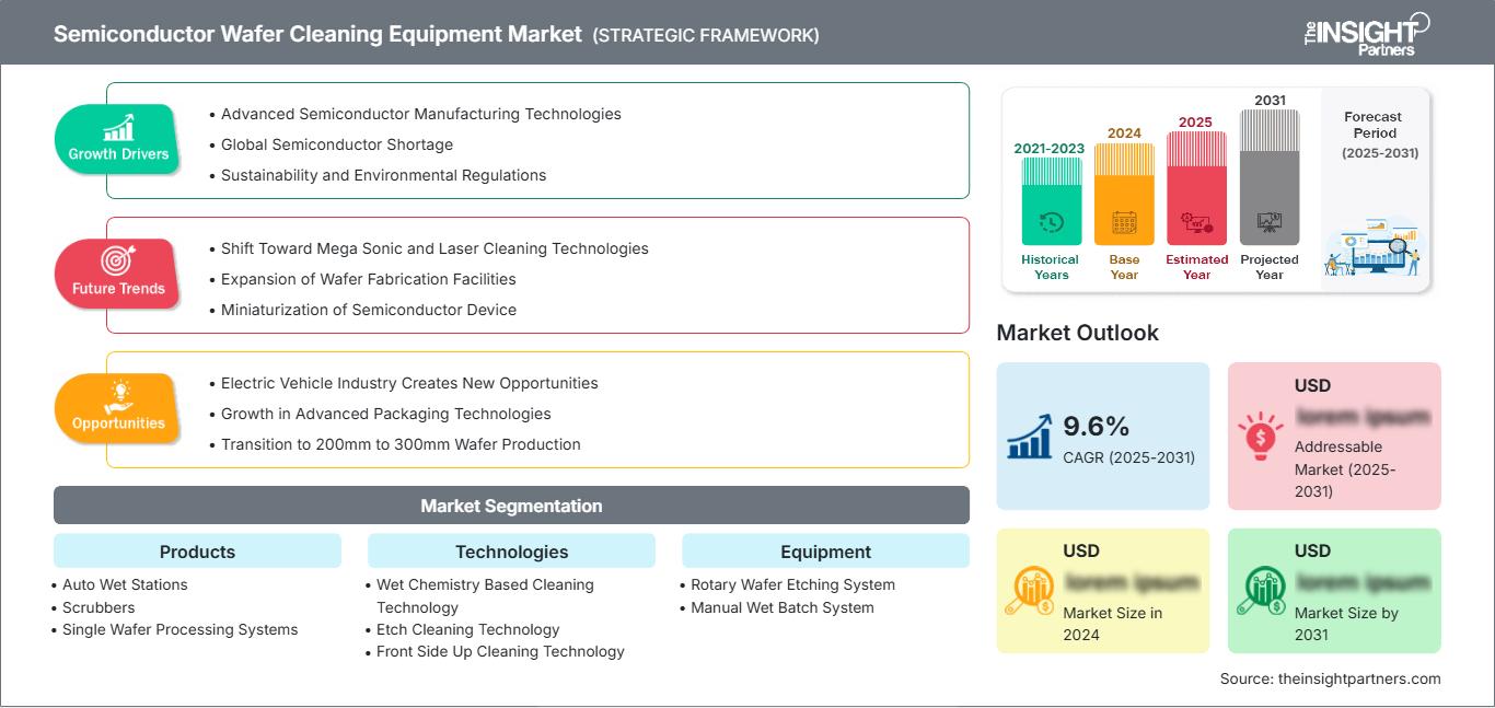
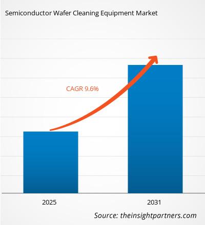
Der globale Markt für Halbleiterwafer-Reinigungsanlagen wird bis 2034 voraussichtlich ein Volumen von 11,58 Milliarden US-Dollar erreichen, gegenüber 8,5 Milliarden US-Dollar im Jahr 2025. Es wird erwartet, dass der Markt im Prognosezeitraum 2026-2034 eine durchschnittliche jährliche Wachstumsrate (CAGR) von 3,94 % verzeichnen wird.
Der Marktbericht für Halbleiterwafer-Reinigungsanlagen umfasst Analysen nach Produkten, Technologien, Anlagen und Endnutzern. Die globale Analyse wird weiter auf regionaler Ebene und für wichtige Länder aufgeschlüsselt. Der Bericht gibt den Wert der oben genannten Analysen und Segmente in US-Dollar an.
Zweck des Berichts
Der Bericht „Markt für Reinigungsanlagen für Halbleiterwafer“ von The Insight Partners beschreibt die aktuelle Marktlage und das zukünftige Wachstum, die wichtigsten Triebkräfte, Herausforderungen und Chancen. Er bietet Einblicke für verschiedene Akteure der Branche, wie zum Beispiel:
- Technologieanbieter/Hersteller: Um die sich entwickelnde Marktdynamik zu verstehen und die potenziellen Wachstumschancen zu erkennen, damit sie fundierte strategische Entscheidungen treffen können.
- Investoren: Um eine umfassende Trendanalyse hinsichtlich der Marktwachstumsrate, der finanziellen Marktprognosen und der Chancen entlang der gesamten Wertschöpfungskette durchzuführen.
- Regulierungsbehörden: Zur Regulierung von Richtlinien und Überwachungstätigkeiten auf dem Markt mit dem Ziel, Missbrauch zu minimieren, das Vertrauen der Anleger zu erhalten und die Integrität und Stabilität des Marktes zu wahren.
Marktsegmentierung für Halbleiterwafer-Reinigungsanlagen
Produkte
- Automatische Nassstationen
- Scheuersaugmaschinen
- Einzelwafer-Verarbeitungssysteme
Technologien
- Nasschemische Reinigungstechnologie
- Ätzreinigungstechnologie
- Reinigungstechnologie mit nach oben gerichteter Vorderseite
Ausrüstung
- Rotations-Wafer-Ätzsystem
- Manuelles Nasschargensystem
Endbenutzer
- Metallische Verunreinigungen
- Chemische Kontamination
- Partikelverunreinigung
Marktanalyse und Einblicke
- Der globale Markt für Halbleiterwafer-Reinigungsanlagen wurde im Jahr 2025 auf 8,50 Milliarden US-Dollar geschätzt.
- Es wird erwartet, dass das jährliche Marktvolumen bis 2034 11,58 Milliarden US-Dollar erreichen wird.
- Der gesamte adressierbare Markt (TAM) wird im Zeitraum 2026-2034 voraussichtlich rund 93,27 Milliarden US-Dollar erreichen.
- Es wird erwartet, dass der Markt im Prognosezeitraum eine durchschnittliche jährliche Wachstumsrate (CAGR) von 3,94 % verzeichnen wird.
- Die Vereinigten Staaten stellen einen Schlüsselmarkt dar, der durch fortschrittliche Halbleiterfertigungstechnologien, den globalen Halbleitermangel, Nachhaltigkeits- und Umweltvorschriften sowie die sich entwickelnde Branchendynamik gestützt wird.
- Die Marktanalyse umfasst Nordamerika, Europa, den asiatisch-pazifischen Raum, Süd- und Mittelamerika, den Nahen Osten und Afrika, wobei das Wachstum über den gesamten Prognosezeitraum bewertet wird.
- Marktchancen wie die Elektrofahrzeugindustrie, die neue Möglichkeiten schafft, das Wachstum bei fortschrittlichen Verpackungstechnologien und der Übergang zur Waferproduktion von 200 mm auf 300 mm werden voraussichtlich die Marktdynamik und den adressierbaren Markt beeinflussen.
- Der Bericht stellt Branchenteilnehmer wie APandS International GmbH, Cleaning Technologies Group, Falcon Process Systems, Lam Research Corporation, Modutek Corporation, ONBoard Solutions Pty Ltd., SCREEN Holdings Co., Ltd., Speedline Technologies, Inc., Tokyo Electron Limited und Veeco Instruments Inc. vor und analysiert Wettbewerbsstrategien und Innovationsentwicklungen.
Passen Sie diesen Bericht Ihren Anforderungen an.
Kostenlose AnpassungMarkt für Halbleiterwafer-Reinigungsanlagen: Strategische Einblicke
-
Ermitteln Sie die wichtigsten Markttrends dieses Berichts.Diese KOSTENLOSE Probe beinhaltet eine Datenanalyse, die von Markttrends bis hin zu Schätzungen und Prognosen reicht.
Wachstumstreiber des Marktes für Halbleiterwafer-Reinigungsanlagen
- Fortschrittliche Halbleiterfertigungstechnologien: Einer der Hauptwachstumstreiber im Markt für Reinigungsanlagen für Halbleiterwafer ist die Nachfrage nach fortschrittlichen Halbleiterfertigungstechnologien. Diese Nachfrage resultiert aus dem Fortschritt hin zu kleineren und komplexeren Chipdesigns, wodurch die Anforderungen an gründliche Reinigungsverfahren zur Herstellung fehlerfreier Wafer steigen. Jüngste Studien prognostizieren, dass die globale Halbleiterindustrie bis 2030 ein Volumen von 1 Billion US-Dollar erreichen könnte, was den Markt für Reinigungsanlagen für Halbleiterwafer deutlich vergrößern dürfte. Dieses Wachstum eröffnet Herstellern wiederum vielfältige Möglichkeiten, Innovationen voranzutreiben und ihre Produktpalette zu erweitern.
- Weltweiter Halbleitermangel: Der anhaltende weltweite Halbleitermangel hat die Investitionen in die Halbleiterfertigung deutlich erhöht. Regierungen und die Privatwirtschaft planen Investitionen in Milliardenhöhe für den Bau neuer Halbleiterfabriken, insbesondere in den USA und Europa. Dieser Boom wirkt sich direkt auf das Wachstum des Marktes für Reinigungsanlagen für Halbleiterwafer aus, da der Bedarf an hochentwickelten Reinigungstechnologien für eine qualitativ hochwertige Produktion in den geplanten Fabriken steigt. Die enorme Nachfrage nach neuen Produktionsanlagen wird sich positiv auf den Marktanteil von Reinigungsanlagen für Halbleiterwafer auswirken.
- Nachhaltigkeit und Umweltauflagen: Strengere Umweltauflagen und ein starker Trend hin zu Nachhaltigkeit sind die wichtigsten Treiber für den Markt für Reinigungsanlagen für Halbleiterwafer. Hersteller setzen verstärkt auf umweltfreundliche Reinigungsverfahren, um die Einhaltung gesetzlicher Bestimmungen zu gewährleisten. Durch die Integration solcher Verfahren eröffnen sich neue Wachstumschancen. Unternehmen, die sich auf nachhaltige Praktiken konzentrieren, werden voraussichtlich einen großen Marktanteil erobern, wie die Marktanalyse für Reinigungsanlagen für Halbleiterwafer zeigt. Weltweit wird zudem verstärkt auf grüne Technologien gesetzt, und die Nachfrage nach umweltfreundlichen Reinigungslösungen wird bis 2026 voraussichtlich um 10 % steigen. Dies unterstreicht den Bedarf an nachhaltigen Innovationen in der Branche.
Markt für Halbleiterwafer-Reinigungsanlagen: Zukunftstrends
- Trend hin zu Ultraschall- und Laserreinigungstechnologien: Der Markt für Anlagen zur Reinigung von Halbleiterwafern verlagert sich hin zu Ultraschall- und Laserreinigungstechnologien. Diese Technologien verbessern die Effizienz und Effektivität der Partikelentfernung und Oberflächenvorbereitung deutlich. Das Marktwachstum dürfte sehr vielversprechend sein und Nordamerika aufgrund seiner technologischen Innovationen einen sehr großen Marktanteil sichern.
- Ausbau der Waferfertigungsanlagen: Der Markt für Reinigungsanlagen für Halbleiterwafer profitiert direkt vom weltweiten Ausbau der Waferfertigungsanlagen, insbesondere angesichts der stetig wachsenden Nachfrage nach Halbleitern. Wesentliche Wachstumstreiber sind die fortschrittliche Halbleiterfertigung für 5G und IoT. Die Trends im Markt für Reinigungsanlagen für Halbleiterwafer zielen auf Investitionen in Reinigungslösungen ab, die hohe Ausbeute und Qualität bieten.
- Miniaturisierung von Halbleiterbauelementen: Die Miniaturisierung von Halbleiterbauelementen hat erhebliche Auswirkungen auf den Markt für Reinigungsanlagen für Halbleiterwafer. Hersteller entwickeln kontinuierlich immer kleinere und gleichzeitig leistungsfähigere Chips, die von gründlichen und präzisen Reinigungsprozessen profitieren, um Qualität und Ausbeute zu gewährleisten. Dieser Trend spiegelt sich auch im Markt für Reinigungsanlagen für Halbleiterwafer wider, wo die Nachfrage nach fortschrittlichen, auf komplexe Designs zugeschnittenen Reinigungstechnologien ein starkes Wachstum antreibt.
Marktchancen für Halbleiterwafer-Reinigungsanlagen
- Die Elektromobilitätsbranche eröffnet neue Chancen: Der Wandel der Automobilindustrie hin zur Elektromobilität treibt die Nachfrage nach hochwertigen Halbleitern an und eröffnet damit neue Möglichkeiten im Markt für Halbleiterwafer-Reinigungsanlagen. Da für die Energieversorgung und Vernetzung von Elektrofahrzeugen fortschrittliche Halbleiterchips benötigt werden, ist die Reinigung von Halbleiterwafern von zentraler Bedeutung. Der Markt für Halbleitermaterialien für Elektrofahrzeuge wird voraussichtlich ein hohes jährliches Wachstum verzeichnen. Der Einsatz fortschrittlicher Packaging-Technologien wie 3D-Stapelung und System-in-Package (SiP) wird zunehmen und dem Markt für Halbleiterwafer-Reinigungsanlagen neue Chancen eröffnen. Diese fortschrittlichen Technologien erfordern extrem saubere Oberflächen, um zuverlässig und leistungsstark zu funktionieren.
- Wachstum bei fortschrittlichen Verpackungstechnologien: Der zunehmende Einsatz fortschrittlicher Verpackungstechnologien wie 3D-Stapelung und System-in-Package (SiP) wird den Markt für Reinigungsanlagen für Halbleiterwafer weiter ankurbeln und neue Chancen eröffnen. Diese Technologien sind hochentwickelt und erfordern äußerst saubere Oberflächen, um zuverlässig und leistungsstark zu funktionieren. Da der Markt für fortschrittliche Verpackungstechnologien bis 2025 voraussichtlich ein Volumen von 60 Milliarden US-Dollar erreichen wird, benötigen Halbleiterhersteller spezialisierte Reinigungslösungen. Unternehmen können Innovationen vorantreiben und einen größeren Marktanteil erobern, indem sie sich auf Erkenntnisse zum Markt für Reinigungsanlagen für Halbleiterwafer im Hinblick auf Verpackungstechnologien konzentrieren.
- Umstellung auf 200-mm- bis 300-mm-Waferproduktion: Die Umstellung des Wafermarktes von 200 mm auf 300 mm verändert den Markt für Reinigungsanlagen für Halbleiterwafer grundlegend. Größere Wafer ermöglichen eine effizientere und kostengünstigere Produktion, wodurch Halbleiterhersteller auf neue Reinigungsanlagen umsteigen. Diese Veränderung auf dem nordamerikanischen Markt für Reinigungsanlagen für Halbleiterwafer ist auf die Bemühungen führender Unternehmen zurückzuführen, die Produktionsprozesse weiterzuentwickeln. Laut Experten wird der Markt für Reinigungsanlagen speziell für 300-mm-Wafer bis 2025 ein enormes Wachstum verzeichnen.
Marktbericht über Reinigungsanlagen für Halbleiterwafer – Umfang
| Berichtattribute | Details |
|---|---|
| Marktgröße im Jahr 2025 | 8,5 Milliarden US-Dollar |
| Marktgröße bis 2034 | 11,58 Milliarden US-Dollar |
| Globale durchschnittliche jährliche Wachstumsrate (2026 - 2034) | 3,94 % |
| Historische Daten | 2021-2024 |
| Prognosezeitraum | 2026–2034 |
| Abgedeckte Segmente |
Nebenprodukte
|
| Abgedeckte Regionen und Länder |
Nordamerika
|
| Marktführer und wichtige Unternehmensprofile |
|
Marktteilnehmerdichte bei Halbleiterwafer-Reinigungsanlagen: Auswirkungen auf die Geschäftsdynamik verstehen
Der Markt für Reinigungsanlagen für Halbleiterwafer wächst rasant, angetrieben durch die steigende Nachfrage der Endverbraucher. Gründe hierfür sind unter anderem sich wandelnde Verbraucherpräferenzen, technologische Fortschritte und ein wachsendes Bewusstsein für die Vorteile der Produkte. Mit steigender Nachfrage erweitern Unternehmen ihr Angebot, entwickeln innovative Lösungen, um den Kundenbedürfnissen gerecht zu werden, und nutzen neue Trends, was das Marktwachstum zusätzlich beflügelt.
Wichtigste Verkaufsargumente
- Umfassende Abdeckung: Der Bericht bietet eine umfassende Analyse der Produkte, Dienstleistungen, Typen und Endnutzer des Marktes für Halbleiterwafer-Reinigungsanlagen und vermittelt so ein ganzheitliches Bild.
- Expertenanalyse: Der Bericht basiert auf dem fundierten Wissen von Branchenexperten und Analysten.
- Aktuelle Informationen: Der Bericht gewährleistet Geschäftsrelevanz durch die Berücksichtigung aktueller Informationen und Datentrends.
- Anpassungsmöglichkeiten: Dieser Bericht kann an die spezifischen Anforderungen des Kunden angepasst werden und sich optimal in die Geschäftsstrategien einfügen.
Der Forschungsbericht zum Markt für Halbleiterwafer-Reinigungsanlagen kann daher maßgeblich dazu beitragen, das Branchenszenario und die Wachstumsaussichten zu entschlüsseln und zu verstehen. Auch wenn einige berechtigte Bedenken bestehen, überwiegen die Vorteile dieses Berichts insgesamt die Nachteile.

Naveen ist ein erfahrener Marktforschungs- und Beratungsexperte mit über 9 Jahren Erfahrung in kundenspezifischen, syndizierten und Beratungsprojekten. In seiner aktuellen Funktion als Associate Vice President hat er erfolgreich Stakeholder entlang der gesamten Projektwertschöpfungskette gemanagt und ist Autor von über 100 Forschungsberichten und über 30 Beratungsaufträgen. Seine Arbeit erstreckt sich auf Industrie- und Regierungsprojekte und trägt maßgeblich zum Kundenerfolg und zur datengesteuerten Entscheidungsfindung bei.
Naveen hat einen Ingenieursabschluss in Elektronik und Kommunikation von der VTU, Karnataka, und einen MBA in Marketing und Operations von der Manipal University. Er ist seit 9 Jahren aktives IEEE-Mitglied und nimmt an Konferenzen und technischen Symposien teil und engagiert sich ehrenamtlich auf Sektions- und regionaler Ebene. Vor seiner aktuellen Position arbeitete er als Associate Strategic Consultant bei IndustryARC und als Industrial Server Consultant bei Hewlett Packard (HP Global).
- Umfassende Analyse der Marktgröße und Prognosen
- Detaillierte Segmentierungsanalyse
- Tiefgehende Bewertung der Marktdynamik
- Einblicke auf regionaler und nationaler Ebene
- Wettbewerbslandschaft und Unternehmens-Benchmarking
- Strategische Business Intelligence
Erfahrungsberichte
Der SCADA-Systemmarktbericht von Insight Partners ist umfassend und bietet wertvolle Einblicke in aktuelle Trends und Zukunftsprognosen. Das Team war durchweg hochprofessionell, reaktionsschnell und hilfsbereit. Wir sind sehr zufrieden und können die Dienstleistungen wärmstens empfehlen.
RAN KEDEM Partner, Reali Technologies LTDsIch habe einen Bericht über einen sehr spezifischen Softwaremarkt angefordert, und das Team hat ihn innerhalb weniger Tage erstellt. Die Informationen waren sehr relevant und gut präsentiert. Anschließend habe ich einige Änderungen und Ergänzungen zum Bericht angefordert. Das Team reagierte erneut sehr schnell, und ich erhielt den Abschlussbericht in weniger als einer Woche.
JEAN-HERVE JENN Vorsitzende, Future AnalyticaWir haben mit The Insight Partners für eine wichtige Marktstudie und Prognose zusammengearbeitet. Sie gaben uns klare Einblicke in Chancen und Risiken, die uns bei der Gestaltung unserer Pläne halfen. Ihre Recherchen waren benutzerfreundlich und basierten auf soliden Daten. Sie halfen uns, kluge und sichere Entscheidungen zu treffen. Wir können sie wärmstens empfehlen.
PIYUSH NAGPAL Sr. Vizepräsident, Fernlicht GlobalDie Insight Partners lieferten aufschlussreiche, gut strukturierte Marktforschung mit fundierter Fachkompetenz. Ihr Team war durchweg professionell und reaktionsschnell. Die benutzerfreundliche Website ermöglichte den Zugriff auf Branchenberichte. Wir empfehlen sie wärmstens für zuverlässige und hochwertige Forschungsdienstleistungen.
YUKIHIKO ADACHI Geschäftsführer, Deep Blue, LLC.Dies ist das erste Mal, dass ich einen Marktbericht von The Insight Partners erworben habe. Obwohl ich zunächst unsicher war, besuchte ich die Website und fühlte mich dann sicherer, das Risiko einzugehen und einen Marktbericht zu kaufen. Ich bin mit der Qualität des Berichts und dem Kundenservice rundum zufrieden. Ich hatte einige Fragen und Anmerkungen zum ersten Bericht, aber nach einigen E-Mail-Gesprächen mit dem Analysten bin ich überzeugt, dass ich einen Bericht habe, den ich als Input für unseren strategischen Planungsprozess verwenden kann. Vielen Dank, dass Sie sich die Zeit genommen und dies zu einer positiven Erfahrung gemacht haben. Ich werde Ihren Service auf jeden Fall weiterempfehlen und Sie werden meine erste Anlaufstelle sein, wenn wir weitere Marktdaten benötigen.
JOHN SUZUKI Präsident und Chief Executive Officer, Vorstandsmitglied, BK TechnologiesIch möchte mich für Ihre Unterstützung und die Professionalität bedanken, die Sie bei der Bearbeitung meiner Informationsanfrage zum IVD-Markt für Infektionskrankheiten in Nigeria gezeigt haben. Ich schätze Ihre Geduld, Ihre Beratung und die Tatsache, dass Sie bereit waren, einen Rabatt anzubieten, der uns schließlich den Abschluss eines Geschäfts ermöglichte. Ich freue mich darauf, The Insight Partners in Zukunft wieder zu beauftragen, dank des Eindrucks, den Sie bei dieser ersten Begegnung bei mir hinterlassen haben.
DR. CHIJIOKE ONYIA GESCHÄFTSFÜHRERIN, PineCrest Healthcare Ltd.Grund zum Kauf
- Fundierte Entscheidungsfindung
- Marktdynamik verstehen
- Wettbewerbsanalyse
- Kundeneinblicke
- Marktprognosen
- Risikominimierung
- Strategische Planung
- Investitionsbegründung
- Identifizierung neuer Märkte
- Verbesserung von Marketingstrategien
- Steigerung der Betriebseffizienz
- Anpassung an regulatorische Trends