
Semiconductor Wafer Cleaning Equipment Market Share, Size & Demand by 2034
Coverage: by Products (Auto Wet Stations, Scrubbers, Single Wafer Processing Systems); Technologies (Wet Chemistry Based Cleaning Technology, Etch Cleaning Technology, Front Side Up Cleaning Technology); Equipment (Rotary Wafer Etching System, Manual Wet Batch System); End Users (Metallic Contamination, Chemical Contamination, Particle Contamination) , and Geography (North America, Europe, Asia Pacific, and South and Central America)
- Status : Data Released
- Report Code : TIPRE00011328
- Category : Electronics and Semiconductor
- No. of Pages : 150
- Available Report Formats :


- Last update date : July 10, 2026


2025 Market Size
US$ 8.5 Bn
Base year value
2034 Forecast
US$ 11.58 Bn
Projected by 2034
CAGR 2026-2034
3.5 %
Growth rate
Addressable Market
US$ 91.22 Bn
(2026-2034)
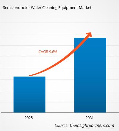
The global Semiconductor Wafer Cleaning Equipment market was valued at US$ 8.5 billion in 2025 and is expected to reach US$ 11.58 billion by 2034; it is estimated to record a CAGR of 3.5% during 2026-2034.
Semiconductor Wafer Cleaning Equipment Market Assessment and Insights
- North America: The region held 24–27% Semiconductor Wafer Cleaning Equipment Market share in 2025 and is growing at a CAGR of 3.6–4.1% during 2026–2034, driven by advanced-node fabs and reshoring incentives.
- US: The US accounted for 78–82% of North America in 2025 and is growing at a CAGR of 3.7–4.2% during 2026–2034 as new fabs expand cleaning demand.
- Europe: Europe held 17–20% share in 2025 and is growing at a CAGR of 3.2–3.8% during 2026–2034, led by Germany, France, Italy, and the UK.
- Asia Pacific: APAC held 48–52% share in 2025 and is growing at a CAGR of 4.1–4.7% during 2026–2034, led by China, Japan, South Korea, and Taiwan-linked supply chains.
- Largest Segment: Single Wafer Processing Systems held 38–42% market share in 2025 and is growing at a CAGR of 4.0–4.6% during 2026–2034.
- High Growth Segment: Wet Chemistry Based Cleaning Technology held 44–48% market share in 2025 and is growing at a CAGR of 4.2–4.8% during 2026–2034.
- Key companies analyzed in detail: AP&S International GmbH, Cleaning Technologies Group, Falcon Process Systems, Lam Research Corporation, Modutek Corporation, ONBoard Solutions Pty Ltd., SCREEN Holdings Co., Ltd., Speedline Technologies, Inc., Tokyo Electron Limited, Veeco Instruments Inc.
Source: The Insight Partners' analysis based on proprietary research, government publications, company annual reports, investor presentations, industry databases, and expert interviews.
Process scaling has made cleaning a critical control point for yield rather than a secondary support process. With the evolution of devices into gate-all-around transistors, 3D NAND stacks, high aspect ratio devices, and heterogenous integration, fabs need better control over particles, metals, and residues. Thus, the expansion of the Semiconductor Wafer Cleaning Equipment Market can be tied to increased cleaning per wafer, reduction of solvent use, megasonics use, and single wafer repeatability.
The Semiconductor Wafer Cleaning Equipment Market forecast indicates that the market will expand due to localized semiconductor manufacturing in India, Southeast Asia, the United States, and Europe. Regulations on water, chemicals, and waste will result in demand for automated wet stations, closed loop chemicals handling, and tools that improve productivity while maintaining defectivity rates.
Semiconductor Wafer Cleaning Equipment Market Report Scope
| Report Attribute | Details |
|---|---|
| Market size in 2025 | US$ 8.5 Billion |
| Market Size by 2034 | US$ 11.58 Billion |
| Global CAGR (2026 - 2034) | 3.5% |
| Historical Data | 2021-2024 |
| Forecast period | 2026-2034 |
Semiconductor Wafer Cleaning Equipment Market Analysis
The demand is driven by the increasing number of cleaning processes necessary for advanced logic, memory, image sensor, power semiconductor, and compound devices. According to SEMI, total front-end fab equipment investment is projected to reach US$110 billion in 2025 and increase to US$130 billion in 2026.
The supply chain comprises suppliers of wet benches, single wafer platforms, chemicals, automation, and fabs with yield learning optimization. The analysis of the Semiconductor Wafer Cleaning Equipment Market reveals that the customer preferences include defectivity, chemical efficiency, availability, versatility of chambers, and compatibility with 300 mm manufacturing processes.
Competitive dynamics focus on the depth of technology and integration into process flows. Lam Research Corporation, SCREEN Holdings Co., Ltd., and Tokyo Electron Limited offer competing advanced single-wafer and batch cleaning systems, while AP&S International GmbH, Modutek Corporation, Cleaning Technologies Group, Falcon Process Systems, ONBoard Solutions Pty Ltd., Speedline Technologies, Inc., and Veeco Instruments Inc. are focused on more narrow wet processing, batch, and specialized applications.
The Semiconductor Wafer Cleaning Equipment Market trends indicate that investments are happening toward tools that reduce the use of water and chemicals while maintaining wafer-level uniformity. Market shares are affected by qualification cycles, installed-base support, and collaboration in the development of advanced fabs. Suppliers having contamination metrology capability, high-speed chambers, and process recipes are most advantaged in equipment selections over multiple years.
● REPORT CUSTOMIZATION
Tailor This Report To Align With Your Specific Business Requirements
This report can be customized to align precisely with your business objectives, scope, and target markets. Customization options include tailored segmentation, geography, competitive analysis, and strategic insights to support informed decision-making.
Customize This Report →WHAT YOU CAN ADJUST
- ● Segmentations
- ● Geography
- ● Competitive Analysis
- ● Language Preferences
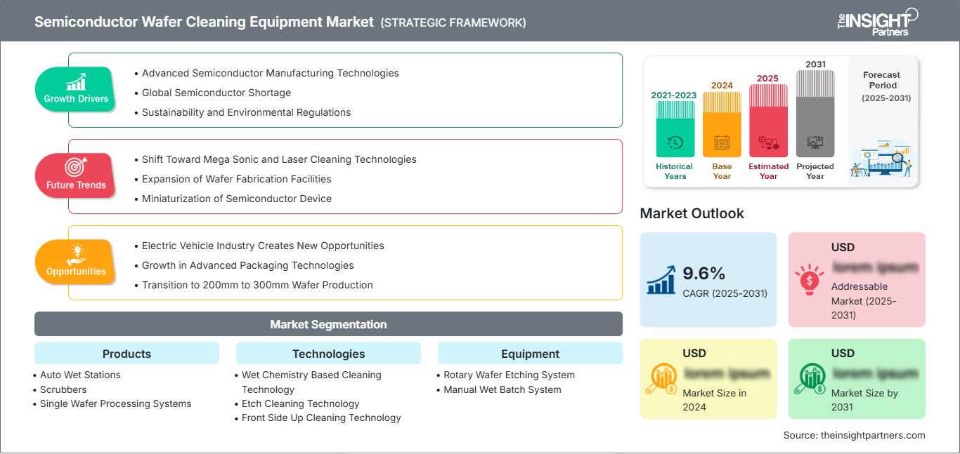
Semiconductor Wafer Cleaning Equipment Market: Strategic Insights
Regional Insights
North America Semiconductor Wafer Cleaning Equipment
North America held 24–27% share in 2025 and is growing at a CAGR of 3.6–4.1% during 2026–2034. Demand is tied to advanced logic, memory packaging, and specialty wafer production. SEMI’s 2025 fab investment outlook highlights sustained front-end spending, strengthening demand for wet cleaning, bevel cleaning, and residue-removal tools.
Regional buyers are emphasizing the need for automation, chemical reclaim, and low-defect process modules to get ready for AI, defense electronics, and automotive chips. There are government incentives for tool localization; however, qualification is taking time since cleaning effectiveness must be demonstrated at the interfaces between etch, CMP, lithography, and deposition processes.
U.S. Semiconductor Wafer Cleaning Equipment Market
The Semiconductor Wafer Cleaning Equipment Market in the US represented 78–82% of North America in 2025 and is growing at a CAGR of 3.7–4.2% during 2026–2034. Fab construction, advanced packaging lines, and materials-equipment funding are creating demand for automated wet stations, scrubbers, and single-wafer systems across logic, analog, and memory-related workflows.
Lam Research Corporation and other equipment suppliers maintain deep customer engagement through process development, service, and installed-base upgrades. US fabs are emphasizing particle contamination, metallic contamination, and chemical contamination control because yield losses at advanced nodes can offset capacity gains. This makes cleaning equipment a strategic purchasing category, not only a facility add-on.
Europe Semiconductor Wafer Cleaning Equipment Market
The Semiconductor Wafer Cleaning Equipment Market in Europe held 17–20% share in 2025 and is growing at a CAGR of 3.2–3.8% during 2026–2034. Germany leads regional demand through automotive semiconductors, power electronics, MEMS, and industrial chips, where reliability requirements increase the importance of wet chemistry control, post-etch cleaning, and low-particle batch processing.
The UK contribution is by means of compound semiconductors, photonics, and R&D pilot lines, which require flexible manual and automatic wet processing. European vendors such as AP&S International GmbH profit from geographical proximity to specialized fabs, though large volume leading-edge requirements are predominantly based in Asia and the US.
France, Italy, and Spain satisfy the Semiconductor Wafer Cleaning Equipment Market requirement through analog, sensors, power devices, and government-funded semiconductor programs. Regulations related to chemical handling and wastewater management motivate investments into better equipment for solvent control. Thus, key trends in Semiconductor Wafer Cleaning Equipment in Europe include process reliability, sustainability, and tool longevity.
APAC Semiconductor Wafer Cleaning Equipment Market
The Semiconductor Wafer Cleaning Equipment Market in APAC held 48–52% share in 2025 and is growing at a CAGR of 4.1–4.7% during 2026–2034. China, Japan, South Korea, India, and Australia support demand through foundries, memory fabs, sensors, and emerging semiconductor ecosystems.
China will continue to be the dominant buyer in the region due to the need for continuous wet clean, scrubbing, and batch cleaning for mature node and specialty processing. Japan will contribute its expertise in equipment and materials. South Korea will contribute on the basis of its expertise in manufacturing memory devices.
India is shifting from design to manufacturing capabilities and will generate initial demand for flexible wet stations and contamination control. Australia will play a smaller role, but one that is related to research and development.
Middle East & Africa Semiconductor Wafer Cleaning Equipment Market
The Semiconductor Wafer Cleaning Equipment Market in Middle East & Africa is growing at a CAGR of 2.6–3.2% during 2026–2034, with Saudi Arabia and the UAE exploring semiconductor-adjacent investments linked to industrial diversification, energy technology, and high-reliability electronics.
The demand base of South Africa and MEA in general is smaller and limited to research, sensors, power devices, and electronics assembly. The demand for cleaning equipment is also selective due to the lack of fully developed ecosystems for the front-end wafer fabrication process.
Potential long-term demand could come from energy infrastructure, data centers, and digital industrial policies that would create a link between electronics manufacturing and localization policies.
Segmentation Analysis
Products
Products are expected to grow at a CAGR of 3.8–4.4% during 2026–2034 as fabs balance batch productivity with single-wafer precision. Adoption depends on wafer size, throughput, contamination type, chemical compatibility, and process-node sensitivity. The Semiconductor Wafer Cleaning Equipment size expansion supports product upgrades that reduce defectivity and improve process repeatability.
- Auto Wet Stations remain important for high-throughput chemical processing, especially where fabs require repeatable batch cleaning, integrated rinsing, and safe handling of acids, solvents, and ultra-pure water.
- Scrubbers address particle-removal requirements in wafer preparation, post-CMP workflows, and specialty production, offering mechanical assistance where surface films and loose particles must be controlled.
- Single Wafer Processing Systems support advanced nodes by enabling tight process control, lower cross-contamination risk, and recipe flexibility for high-value wafers in logic, memory, and packaging.
Technologies
The technologies segment in the Semiconductor Wafer Cleaning Equipment Market is expected to grow at a CAGR of 4.0–4.6% during 2026–2034 as contamination-control recipes become more application-specific. Wet chemistry remains dominant, while etch cleaning and front side up cleaning address increasingly fragile surfaces. Tool suppliers are differentiating through reduced chemical usage, drying performance, and surface-loss control.
- Wet Chemistry Based Cleaning Technology is strategically important because chemical selectivity, rinse control, and drying quality directly influence wafer yield across memory, logic, MEMS, and power semiconductor production.
- Etch Cleaning Technology supports residue removal after plasma and wet etch steps, helping fabs manage polymers, metals, and films without damaging increasingly narrow device features.
- Front Side Up Cleaning Technology improves control of active wafer surfaces, supporting applications where particle redeposition, pattern collapse, and surface roughness must be tightly managed.
Equipment
Equipment segment in the Semiconductor Wafer Cleaning Equipment Market is expected to grow at a CAGR of 3.5–4.1% during 2026–2034 as manufacturers seek flexible systems for etching, rinsing, drying, and batch processing. Demand spans advanced fabs and specialty lines where capital intensity, operator safety, and chemical process consistency influence purchasing decisions.
- Rotary Wafer Etching System demand is linked to controlled material removal, uniform surface conditioning, and process flexibility for applications requiring repeatable etch profiles.
- Manual Wet Batch System remains relevant for research, pilot production, specialty wafers, and lower-volume fabs that need configurable cleaning without full automation investment.
End Users
End Users are expected to grow at a CAGR of 3.7–4.3% during 2026–2034 as fabs classify cleaning needs by contamination source and yield impact. Metallic, chemical, and particle contamination each require distinct process recipes, inspection integration, and equipment controls to maintain device reliability.
- Metallic Contamination control is critical for advanced devices because trace metals can alter electrical behavior, reduce reliability, and compromise performance in logic, memory, and power applications.
- Chemical Contamination management supports process stability by removing residues from etch, deposition, lithography, and CMP steps while avoiding surface damage or unwanted material loss.
- Particle Contamination remains a high-priority use case because nanoscale particles can create defects, lower yield, and disrupt patterning accuracy in advanced semiconductor production.
Opportunity Snapshot
| Segment Name | Revenue Contribution | Trend Tag | Adoption Stage |
| Metallic Contamination | High | Trace Metals | Mature |
| Chemical Contamination | Medium | Residue Control | Scaling |
| Particle Contamination | High | Nanoscale Defects | Mature |
Semiconductor Wafer Cleaning Equipment Market Growth Drivers and Impact Analysis
Advanced Node Defect Sensitivity
With the continued miniaturization and three-dimensional nature of transistors, even small particles, residues, or metal contaminations may adversely affect yield. Advanced logic devices, 3D NAND, imaging sensors, and high-bandwidth memory need more cleaning steps and tighter processing windows. In turn, there is a greater need for single-wafer, wet-chemistry, and scrubbing solutions that can help remove defects without harming the fragile transistors. The result is clear: cleaning equipment becomes more dependent not just on price, but on its yield contribution and process repeatability.
Fab Regionalization and Capacity Additions
Governments and semiconductor manufacturers are investing to secure chip supplies for AI, automotive, industrial, and defense electronics by building regional semiconductor plants. According to SEMI projections regarding investment in front-end fab equipment, there will be high capital expenditure, which means that new fabs and expansions will involve purchasing full contamination control toolset. The cleaning equipment is positively affected due to the fact that all process modules need surface preparation and defects reduction.
Chemical Efficiency and Sustainability Requirements
Wafer cleaning consumes chemicals, ultra-pure water, energy, filters, and waste-treatment capacity, making sustainability a purchasing factor. Fabs are increasingly selecting tools that improve rinse efficiency, reclaim solvents, reduce chemical drag-out, and support safer handling. Environmental requirements in Europe, North America, Japan, and South Korea reinforce this shift. The market impact is a stronger replacement cycle for platforms that lower operating costs while maintaining high defect-removal performance, especially in high-volume 300 mm production.
Semiconductor Wafer Cleaning Equipment Market Future Trends
AI-Driven Process Control
Future cleaning platforms will increasingly integrate sensor data, recipe analytics, and predictive maintenance to reduce excursion risk. AI-enabled process control can connect particle maps, chemical concentration, chamber condition, and yield data, allowing fabs to adjust cleaning recipes faster. This trend will be particularly valuable for high-mix fabs and advanced packaging lines where contamination sources vary by product. Vendors that combine equipment hardware with analytics and service models will strengthen customer lock-in over the forecast period.
Cleaning for Heterogeneous Integration
Advanced packaging, chiplets, wafer bonding, and hybrid integration are changing cleaning requirements beyond traditional front-end steps. Surfaces must be prepared for bonding, metallization, redistribution layers, and temporary carrier handling, often with tighter control over organic residues and particles. The trend will expand demand for flexible wet cleaning and drying systems that support diverse materials. Equipment suppliers able to address both front-end and packaging interfaces will capture broader customer spending.
Semiconductor Wafer Cleaning Equipment Market Opportunities
Localized Service and Retrofit Programs
Tool suppliers can expand revenue by offering retrofit kits, chamber upgrades, chemical-delivery improvements, and regional service capacity for installed wet cleaning platforms. Many fabs operate mixed tool generations, and targeted upgrades can improve defectivity, uptime, and sustainability without full replacement. This opportunity is attractive in mature-node, power, MEMS, and specialty fabs where capital discipline is high. Strong local service teams also reduce downtime risk, improving supplier preference during future equipment selections.
India and Southeast Asia Pilot-Line Demand
Emerging semiconductor ecosystems in India and Southeast Asia create opportunities for modular wet benches, manual batch systems, training-oriented platforms, and scalable automation. Early fabs, outsourced assembly operations, R&D centers, and compound-semiconductor pilots need flexible equipment before committing to high-volume configurations. Suppliers that support process transfer, operator training, and chemical safety can shape early customer standards. This creates a pathway from pilot adoption to larger production awards as regional manufacturing maturity improves.
Recent Developments
- September 2025: SCREEN Semiconductor Solutions Co., Ltd. – entered into an agreement with IBM to develop cleaning technology for future-generation EUV lithography, including high NA EUV. This joint effort focuses on particle and scratch control in sub-2nm production utilizing IBM’s process integration know-how with SCREEN’s wafer cleaning equipment.
- November 2025: RENA Technologies launched of Vanguard. It is an innovative, fully automated single wafer system designed to clean, etch, and dry 200mm and 300mm wafers using wet chemistry technology. The versatile Vanguard provides a whole new range of opportunities in advanced semiconductor processing.
- October 2025: Spending on 300mm fabs equipment has been forecasted to rise to US$374 billion in 2026 to 2028, according to SEMI in the recent 300mm Fab Outlook report published. The aforementioned spending forecast drives demand for contamination control equipment, including wafer cleaning system
Frequently Asked Questions

- Comprehensive Market Sizing and Forecast Analysis
- Detailed Segmentation Analysis
- In-Depth Market Dynamics Assessment
- Regional and Country-Level Insights
- Competitive Landscape and Company Benchmarking
- Strategic Business Intelligence
Recent Reports
Testimonials

The Insight Partners provided valuable market intelligence that supported our global go-to-market strategy. Their team was professional, responsive, and attentive to our feedback, providing thoughtful analysis and helpful methodological clarifications throughout the project.
Junmo Kim Chief Financial Officer (CFO), Enertech Co., Ltd.
The Insight Partners' SCADA System Market report is comprehensive, with valuable insights on current trends and future forecasts. The team was highly professional, responsive, and supportive throughout. We are very satisfied and highly recommend their services.
RAN KEDEM Partner, Reali Technologies LTDs
I requested a report on a very specific software market and the team produced the report in a few days. The information was very relevant and well presented. I then requested some changes and additions to the report. The team was again very responsive and I got the final report in less than a week.
JEAN-HERVE JENN Chairman, Future Analytica
We worked with The Insight Partners for an important market study and forecast. They gave us clear insights into opportunities and risks, which helped shape our plans. Their research was easy to use and based on solid data. It helped us make smart, confident decisions. We highly recommend them.
PIYUSH NAGPAL Sr. Vice President, High Beam Global
The Insight Partners delivered insightful, well-structured market research with strong domain expertise. Their team was professional and responsive throughout. The user-friendly website made accessing industry reports seamless. We highly recommend them for reliable, high-quality research services
YUKIHIKO ADACHI CEO, Deep Blue, LLC.
This is the first time I have purchased a market report from The Insight Partners.While I was unsure at first, I visited their web site and felt more comfortable to take the risk and purchase a market report.I am completely satisfied with the quality of the report and customer service. I had several questions and comments with the initial report, but after a couple of dialogs over email with their analyst I believe I have a report that I can use as input to our strategic planning process.Thank you so much for taking the extra time and making this a positive experience.I will definitely recommend your service to others and you will be my first call when we need further market data.
JOHN SUZUKI President and Chief Executive Officer, Board Director, BK Technologies
I wish to appreciate your support and the professionalism you displayed in the course of attending to my request for information regarding to infectious disease IVD market in Nigeria. I appreciate your patience, your guidance, and the fact that you were willing to offer a discount, which eventually made it possible for us to close a deal. I look forward to engaging The Insight Partners in the future, all thanks to the impression you have created in me as a result of this first encounter.
DR CHIJIOKE ONYIA MANAGING DIRECTOR, PineCrest Healthcare Ltd.Reason to Buy
- Informed Decision-Making
- Understanding Market Dynamics
- Competitive Analysis
- Identifying Emerging Markets
- Customer Insights
- Market Forecasts
- Risk Mitigation
- Boosting Operational Efficiency
- Strategic Planning
- Investment Justification
- Tracking Industry Innovations
- Aligning with Regulatory Trends





 Get Free Sample for