
Advanced Packaging Market Trends, Demand & Growth by 2034
Coverage: By Technology (Wafer-level Chip-scale Packaging, 3D Integrated Circuit Packaging, Silicon in Package, 3D Wafer level Package, 2.5 D, Flip Chip); and Application (Consumer Electronics, Automotive, IT & Telecommunication, Healthcare, Aerospace & Defense, and Others), and Geography (North America, Europe, Asia Pacific, and South and Central America)
- Status : Data Released
- Report Code : TIPEL00002151
- Category : Electronics and Semiconductor
- No. of Pages : 150
- Available Report Formats :


- Last update date : July 09, 2026


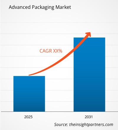
2025 Market Size
US$ 43.95 Bn
Base year value
2034 Forecast
US$ 69.71 Bn
Projected by 2034
CAGR 2026-2034
5.26 %
Growth rate
Addressable Market
US$ 515.60 Bn
(2026-2034)
The Advanced Packaging Market was valued at US$ 43.95 Billion in 2025 and is projected to reach US$ 69.71 Billion by 2034, growing at a CAGR of 5.26% during 2026–2034. The Advanced Packaging Market is expanding as chipmakers use heterogeneous integration, wafer-level formats, flip chip, silicon interposers, and system-in-package designs to improve performance, reduce footprint, manage power, and extend semiconductor scaling beyond front-end node advances.
North America is expected to grow at a CAGR range of 5.0–5.4% during 2026–2034 as domestic semiconductor investment, AI accelerator packaging, defense electronics, and automotive electrification strengthen regional demand. U.S. CHIPS programs, substrate research, and high-volume packaging plans are improving ecosystem depth, while advanced packaging demand remains tied to high-performance computing, communications infrastructure, and resilient supply chain strategies.
Advanced Packaging Market Assessment and Insights
- North America: The region holds 24–28% share in 2025 and grows at a CAGR of 5.0–5.4% during 2026–2034, supported by AI infrastructure, substrate R&D, and domestic packaging investments.
- US: The country represents 76–80% of North America in 2025 and grows at a CAGR of 5.1–5.5% during 2026–2034, led by advanced nodes, defense electronics, and packaging campuses.
- Europe: The region accounts for 18–22% share in 2025 and grows at a CAGR of 4.6–5.0% during 2026–2034, with Germany, France, the UK, Italy, and Spain leading automotive and industrial demand.
- Asia Pacific: The region holds 48–52% share in 2025 and grows at a CAGR of 5.5–5.9% during 2026–2034, led by Taiwan, South Korea, China, Japan, and India across foundry, OSAT, and electronics clusters.
- Largest Segment: Flip Chip holds 38–42% market share in 2025 and grows at a CAGR of 4.8–5.2% during 2026–2034 because it supports high I/O density, thermal efficiency, and mature volume manufacturing.
- High Growth Segment: 3D Integrated Circuit Packaging holds 10–14% market share in 2025 and grows at a CAGR of 6.6–7.0% during 2026–2034 as chiplet, memory stacking, and AI accelerator needs intensify.
- Key companies analyzed in detail: Amkor Technology, Inc.; ASE Technology Holding Co., Ltd.; Intel Corporation; International Business Machines Corporation; Qualcomm Incorporated; Semiconductor Manufacturing International Corporation; JCET Group Co., Ltd.; SÜSS MicroTec SE; Taiwan Semiconductor Manufacturing Company Limited; United Microelectronics Corporation; Samsung Electronics Co., Ltd.
Source: The Insight Partners' analysis based on proprietary research, government publications, company annual reports, investor presentations, industry databases, and expert interviews.
Advanced packaging has transitioned from being a back-end process to becoming a performance factor for semiconductors. The industry is developing itself via improvements in redistribution layers, silicon interposers, hybrid bonding, fan-out configurations, and substrates that will be used for chiplets. The industry dynamics are driven by long lead times for equipment, limitations in substrates, warpage issues, testing complications, and an increased need for co-packaged memory in artificial intelligence accelerators, HPC, 5G, automotive, and premium devices.
Forward-looking demand will be concentrated in Asia Pacific manufacturing ecosystems, U.S. reshoring projects, and European automotive semiconductor programs. The Advanced Packaging Market scope is widening as governments treat packaging as strategic infrastructure, not a low-value assembly stage. Investment will favor high-density substrates, panel-level processes, advanced thermal materials, and known-good-die testing that improves yield before expensive multi-die integration.
Advanced Packaging Market Report Scope
| Report Attribute | Details |
|---|---|
| Market size in 2025 | US$ 43.95 Billion |
| Market Size by 2034 | US$ 69.71 Billion |
| Global CAGR (2026 - 2034) | 5.26% |
| Historical Data | 2021-2024 |
| Forecast period | 2026-2034 |
Advanced Packaging Market Analysis
The demand arises from the economics of transistor scaling slowdown, an increase in bandwidth needs, and integration of logic, memory, radio frequency, power management, and sensor devices into smaller form factors. AI processing involves short distances of interconnection and proximity to high bandwidth memories, whereas thin form factor and efficient power consumption are a must in the case of smartphones and wearable devices.
The value chain includes wafer foundries, OSAT providers, substrate suppliers, equipment vendors, materials companies, EDA providers, test houses, and fabless chip designers. Supply dynamics are increasingly capacity-sensitive because advanced packaging lines require cleanroom space, lithography, bonding, plating, underfill, metrology, and thermal process expertise. Advanced Packaging Market analysis indicates that yield learning and design co-optimization now influence customer sourcing decisions as much as unit assembly cost.
The competitive environment consists of foundry, IDM, and OSAT firms with varying strengths in their strategies. Taiwan Semiconductor Manufacturing Company Limited is the leader for premium CoWoS, InFO, and SoIC platforms. ASE Technology Holding Co., Ltd. and Amkor Technology, Inc. offer scale and broad customer reach and outsourcing capabilities. Intel Corporation emphasizes EMIB and Foveros technology, whereas Samsung Electronics Co., Ltd. has increased its offerings of memory-based and 2.5D/3D integration.
Investment trends indicate that investment has moved away from traditional assembly capacity to heterogeneous integration infrastructure. For instance, Amkor Technology, Inc. has increased its investments in U.S. advanced packaging services, ASE Technology Holding Co., Ltd. is increasing its capabilities in relation to artificial intelligence. At the same time, SÜSS MicroTec SE benefits from the need for temporary bonding, lithography, and wafer processing equipment. There are also chip design firms like Qualcomm Incorporated, International Business Machines Corporation, Semiconductor Manufacturing International Corporation, JCET Group Co., Ltd., and United Microelectronics Corporation.
● REPORT CUSTOMIZATION
Tailor This Report To Align With Your Specific Business Requirements
This report can be customized to align precisely with your business objectives, scope, and target markets. Customization options include tailored segmentation, geography, competitive analysis, and strategic insights to support informed decision-making.
Customize This Report →WHAT YOU CAN ADJUST
- ● Segmentations
- ● Geography
- ● Competitive Analysis
- ● Language Preferences
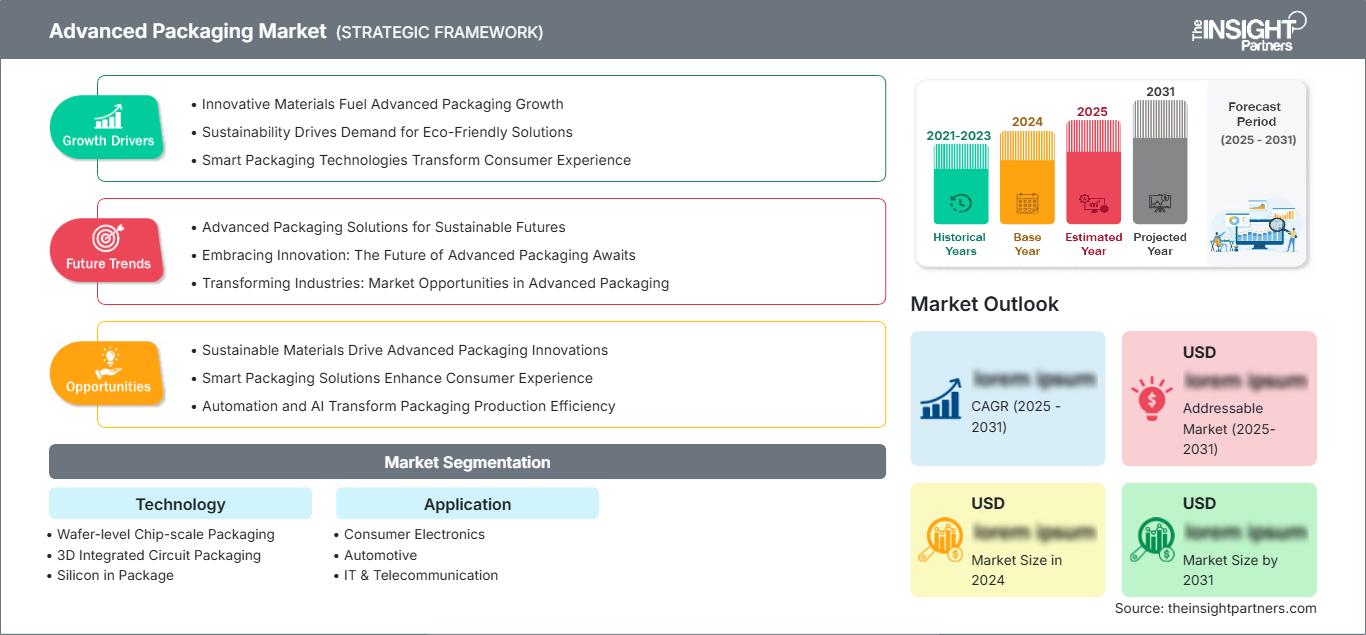
Advanced Packaging Market: Strategic Insights
Regional Insights
North America Advanced Packaging Market
North America holds 24–28% share in 2025 and is projected to grow at a CAGR of 5.0–5.4% during 2026–2034. Demand is supported by AI accelerator design, defense electronics, automotive semiconductors, and data center processors that require higher interconnect density. U.S. policy support for substrates and packaging pilots is strengthening the domestic ecosystem, while large fab investments increase the need for nearby packaging and test capacity.
The region’s Advanced Packaging Market share is also supported by fabless semiconductor leadership, EDA strength, and customers that need secure supply chains. Growth is limited by workforce gaps, substrate availability, and the time required to qualify high-volume facilities. However, the long-term outlook is improving as foundry, OSAT, equipment, and materials companies align around domestic assembly, test, and advanced package validation.
U.S. Advanced Packaging Market
The U.S. represents 76–80% of North American demand in 2025 and is expected to grow at a CAGR of 5.1–5.5% during 2026–2034. The country benefits from AI chip design, defense-grade electronics, cloud infrastructure investment, and emerging high-volume packaging campuses. Amkor Technology, Inc., Intel Corporation, International Business Machines Corporation, Qualcomm Incorporated, and Taiwan Semiconductor Manufacturing Company Limited support the ecosystem through packaging, process, design, and research activity.
Application trends are strongest in high-performance computing, aerospace and defense, telecommunications, and automotive platforms. Packaging demand is shifting toward 2.5D integration, fan-out, flip chip, and chiplet-based architectures that reduce latency and improve power efficiency. The Advanced Packaging Market size in the U.S. is also supported by public-private programs targeting substrates, thermal management, test methods, and workforce development.
Europe Advanced Packaging Market
Europe accounts for 18–22% share in 2025 and is forecast to grow at a CAGR of 4.6–5.0% during 2026–2034. Germany is the leading country because automotive electronics, industrial automation, power semiconductors, and research institutes create sustained demand. The UK contributes through compound semiconductors, photonics, defense electronics, and design services that require specialized assembly routes.
In addition to aerospace and defense applications, France has added capabilities in smart card and microelectronic packaging. Meanwhile, Italy and Spain have also provided support in automotive, industrial, telecommunication, and power electronic packaging projects. The reliability, traceability, and thermal performance issues are highly important for European consumers due to the nature of their application areas. This makes flip chip, SIP, and 2.5D packaging more relevant to these applications.
Advanced Packaging Market trends in Europe are influenced by semiconductor sovereignty, energy efficiency, and electrification. Regional investments prioritize pilot lines, R&D centers, and packaging for automotive, industrial, and aerospace use rather than pure consumer electronics volume. Suppliers with strong quality systems, materials knowledge, and equipment capability are well-positioned as Europe aligns chip design, wafer processing, and package qualification.
APAC Advanced Packaging Market
Asia Pacific holds 48–52% share in 2025 and is projected to grow at a CAGR of 5.5–5.9% during 2026–2034. Taiwan leads through foundry-linked advanced packaging, OSAT depth, and AI accelerator demand.
Korea focuses on the memory-centric 2.5D and 3D integrations; China builds capabilities for outsourcing assembly and testing, consumer electronics packaging, and semiconductor production within its own country, whereas Japan provides advanced materials, equipment, and substrates required for fine-pitch manufacturing.
India is emerging through electronics manufacturing, semiconductor policy, and design activity, while Australia remains smaller but relevant for defense, research, and specialty electronics. Industrial clusters and policy incentives make APAC central to the Advanced Packaging Market growth.
Middle East & Africa Advanced Packaging Market
The Middle East & Africa market is forecast to grow at a CAGR of 4.2–4.6% during 2026–2034. Saudi Arabia is the leading country in digital infrastructure, defense localization, and smart city programs, which increases demand for advanced electronics.
The United Arab Emirates participates in adoption through data centers, aerospace, telecoms, and electronics distribution channels. The contribution of South Africa will be through industrial automation, mining technology, defense electronics, and university-based engineering activities, which require the packaging of semiconductor devices.
Demand from the rest of the MEA region will be import-driven and project-based. Growth will be contingent upon assembly alliances, manpower availability, testing, and integration with energy, telecom, and infrastructure projects.
Segmentation Analysis
Technology
The technology segment is projected to grow at a CAGR of 5.1–5.5% during 2026–2034. Adoption is shaped by die size, interconnect density, power delivery, thermal requirements, manufacturing yield, and cost sensitivity. Flip chip remains the volume anchor, while 2.5D and 3D approaches are gaining importance for AI, high-bandwidth memory, and chiplet architectures. Wafer-level formats support compact consumer and mobile devices.
- Wafer-level Chip-scale Packaging: This sub-segment serves smartphones, wearables, sensors, and compact modules where small footprint, short interconnects, and efficient batch processing support high-volume cost targets.
- 3D Integrated Circuit Packaging: This sub-segment is strategically important for stacking logic, memory, and functional dies, improving bandwidth and footprint where performance density justifies higher design and process complexity.
- Silicon in Package: This sub-segment integrates multiple functions in one package, supporting mobile, telecom, automotive, and IoT products that require compact layouts, power efficiency, and faster system-level design cycles.
- 3D Wafer level Package: This sub-segment supports vertically integrated wafer-scale structures where miniaturization, signal speed, and assembly precision are critical for advanced sensors, imaging devices, and compact electronic systems.
- 2.5 D: This sub-segment uses interposers or bridges to connect logic and memory dies, making it essential for AI accelerators, high-performance computing, networking chips, and bandwidth-intensive processors.
- Flip Chip: This sub-segment remains the largest technology because it offers high I/O density, strong electrical performance, and mature manufacturing economics across processors, mobile chips, automotive electronics, and communications devices.
Application
The application segment is expected to grow at a CAGR of 5.2–5.6% during 2026–2034. Consumer electronics remain broad, but growth increasingly comes from compute-heavy devices, electric vehicles, 5G infrastructure, medical equipment, and aerospace systems. The Advanced Packaging Market forecast indicates the strongest growth outlook in applications where performance, power, and space constraints require chiplets, high-bandwidth memory, fan-out routing, or ruggedized system-in-package solutions.
- Consumer Electronics: Demand is led by smartphones, tablets, wearables, gaming devices, and laptops, where thinner designs, better battery life, higher processing power, and camera performance require compact advanced packages.
- Automotive: Adoption is rising across ADAS, infotainment, power management, vehicle connectivity, and electric drivetrains, where reliability, thermal control, and miniaturized electronics are key design priorities.
- IT & Telecommunication: This sub-segment drives high-value demand through AI servers, networking ASICs, 5G equipment, optical modules, and high-performance processors requiring dense interconnects and efficient signal routing.
- Healthcare: Medical imaging, implantable devices, diagnostics, monitoring equipment, and connected instruments use advanced packaging to support miniaturization, low power consumption, reliability, and precise sensor integration.
- Aerospace & Defense: Demand is supported by radar, satellites, secure communications, avionics, and mission electronics, where rugged packages, thermal stability, and long qualification cycles influence supplier selection.
Opportunity Snapshot
| Application | Revenue Contribution | Trend Tag | Adoption Stage |
| Consumer Electronics | High | Compact Devices | Mature |
| Automotive | Medium | ADAS Modules | Scaling |
| IT & Telecommunication | High | AI Servers | Scaling |
| Healthcare | Medium | Mini Sensors | Scaling |
| Aerospace & Defense | Medium | Rugged Chips | Emerging |
Advanced Packaging Market Growth Drivers and Impact Analysis
AI Accelerators Requiring Dense Memory Integration
AI training and inference systems require extremely high data movement between logic and memory, making advanced packaging essential rather than optional. 2.5D interposers, high-bandwidth memory integration, and chiplet architectures reduce electrical distance, improve bandwidth, and manage power more effectively than board-level approaches. The Advanced Packaging Market is benefiting from capacity expansion for CoWoS-like platforms, substrate demand, thermal materials, and advanced testing. Suppliers that can deliver high yield, large package formats, and reliable warpage control gain stronger bargaining power with cloud processor, GPU, and custom ASIC customers.
Chiplet Architectures Extending Semiconductor Scaling Economics
Chiplets allow designers to combine dies made on different process nodes, improving cost, yield, and design flexibility. Instead of building a very large monolithic die, companies can partition compute, memory, I/O, analog, and security functions into optimized blocks. Advanced packaging provides the interconnect layer that makes this architecture practical. The market impact is higher demand for design co-optimization, known-good-die testing, interposer substrates, and package-level simulation. The Advanced Packaging Market is benefiting from this shift in value toward companies that can support co-design across wafer fabrication, package layout, thermal behavior, and final system validation.
Automotive Electronics Becoming More Compute Intensive
Semiconductor content per vehicle has increased due to electric vehicles, driver assistance technology, software-defined architecture in vehicles, and in-vehicle connectivity. Advanced packaging allows for the integration of processors, sensors, power management, and communication chips in small packages that have high reliability standards. The effect on the industry is gradual but consistent since qualification cycles in the automotive industry take a long time, and win design cycles last for many years. Those suppliers with good thermal management, traceability, and failure analysis are well-positioned to capitalize on the market trend.
Advanced Packaging Market Future Trends
Hybrid Bonding Moving Toward Broader Production Use
Hybrid bonding will likely be shifted to more widespread usage from selective usage at a premium end due to the smaller pitch needed between die-to-die interconnects. This technology has the potential to increase bandwidth and reduce power consumption by bonding copper and dielectric surfaces without using bumps. The success during the forecast period will be determined by factors such as surface preparation, cleanliness, precision in alignment, inspection, and repair methods. Improved yield will make hybrid bonding a major player in the 3D logic stacking, image sensing, and memory-on-logic technologies.
Panel-Level Packaging Pursuing Cost and Scale Advantages
Panel-level packaging is gaining attention because larger processing areas can improve throughput and reduce cost if yield, warpage, and equipment standardization challenges are controlled. The approach is attractive for fan-out, power devices, automotive modules, and selected AI-related packages that need more economical redistribution processing. Future adoption will be uneven because panel formats require new process controls and customer qualification. However, companies that master materials handling, lithography uniformity, and inspection across larger panels can create a cost advantage in high-volume applications.
Advanced Packaging Market Opportunities
Domestic Packaging Ecosystems for Strategic Semiconductors
Governments and customers are looking beyond wafer fabrication to ensure that advanced chips can be packaged, tested, and qualified close to strategic markets. This creates an opportunity for OSAT providers, substrate makers, tool suppliers, universities, and system integrators to build localized ecosystems. The action path includes pilot lines, workforce training, shared reliability labs, and qualification programs for AI, defense, automotive, and telecom devices. Companies that participate early can secure anchor customers, reduce supply risk, and position themselves for long-cycle public and private investment.
Thermal Management Materials and Package Co-Design
Higher power density is making heat removal a central constraint in advanced packaging. This creates investment opportunities in thermal interface materials, heat spreaders, embedded cooling structures, low-warpage substrates, and simulation-led package design. Suppliers can differentiate by solving thermal, mechanical, and electrical trade-offs together rather than selling standalone materials. The opportunity is strongest in AI accelerators, networking processors, automotive power electronics, and aerospace systems, where overheating affects performance, reliability, and warranty exposure. Co-design services can also create stickier customer relationships.
Recent Developments
- September 2025: FUJIFILM Corporation announced the launch of CMP slurry*1 for advanced packaging, enabling the integration of multiple semiconductor chips into a single package. This product has been adopted by a major semiconductor device manufacturer as an essential abrasive for planarizing bonding surfaces in hybrid bonding*2, one of the advanced packaging technologies key to enhancing AI semiconductor performance.
- June 2026: Qnity Electronics, Inc., a premier technology solutions leader across the semiconductor value chain, today introduced enhanced advanced packaging material solutions for organic interposer applications: Intervia 8540HSP multi-role copper and Cyclotene DF6800M dry film photo-imageable dielectric. The material innovations are designed to support advanced interconnect formation, redistribution layer (RDL) designs, and emerging glass-based substrate structures.
- February 2026: ACM Research, Inc. (“ACM”), a leading supplier of wafer and panel processing solutions for semiconductor and advanced packaging applications, today announced it has received multiple advanced packaging equipment orders from leading global semiconductor and technology customers.
Frequently Asked Questions

- Comprehensive Market Sizing and Forecast Analysis
- Detailed Segmentation Analysis
- In-Depth Market Dynamics Assessment
- Regional and Country-Level Insights
- Competitive Landscape and Company Benchmarking
- Strategic Business Intelligence
Recent Reports
Testimonials

The Insight Partners' SCADA System Market report is comprehensive, with valuable insights on current trends and future forecasts. The team was highly professional, responsive, and supportive throughout. We are very satisfied and highly recommend their services.
RAN KEDEM Partner, Reali Technologies LTDs
I requested a report on a very specific software market and the team produced the report in a few days. The information was very relevant and well presented. I then requested some changes and additions to the report. The team was again very responsive and I got the final report in less than a week.
JEAN-HERVE JENN Chairman, Future Analytica
We worked with The Insight Partners for an important market study and forecast. They gave us clear insights into opportunities and risks, which helped shape our plans. Their research was easy to use and based on solid data. It helped us make smart, confident decisions. We highly recommend them.
PIYUSH NAGPAL Sr. Vice President, High Beam Global
The Insight Partners delivered insightful, well-structured market research with strong domain expertise. Their team was professional and responsive throughout. The user-friendly website made accessing industry reports seamless. We highly recommend them for reliable, high-quality research services
YUKIHIKO ADACHI CEO, Deep Blue, LLC.
This is the first time I have purchased a market report from The Insight Partners.While I was unsure at first, I visited their web site and felt more comfortable to take the risk and purchase a market report.I am completely satisfied with the quality of the report and customer service. I had several questions and comments with the initial report, but after a couple of dialogs over email with their analyst I believe I have a report that I can use as input to our strategic planning process.Thank you so much for taking the extra time and making this a positive experience.I will definitely recommend your service to others and you will be my first call when we need further market data.
JOHN SUZUKI President and Chief Executive Officer, Board Director, BK Technologies
I wish to appreciate your support and the professionalism you displayed in the course of attending to my request for information regarding to infectious disease IVD market in Nigeria. I appreciate your patience, your guidance, and the fact that you were willing to offer a discount, which eventually made it possible for us to close a deal. I look forward to engaging The Insight Partners in the future, all thanks to the impression you have created in me as a result of this first encounter.
DR CHIJIOKE ONYIA MANAGING DIRECTOR, PineCrest Healthcare Ltd.Reason to Buy
- Informed Decision-Making
- Understanding Market Dynamics
- Competitive Analysis
- Identifying Emerging Markets
- Customer Insights
- Market Forecasts
- Risk Mitigation
- Boosting Operational Efficiency
- Strategic Planning
- Investment Justification
- Tracking Industry Innovations
- Aligning with Regulatory Trends





 Get Free Sample for