
Back End of the Line Semiconductor Equipment Market Share, Growth & Demand by 2034
Coverage: by Product Type (CVD, Coater Developer, CMP, Metal Etching, PVD, Wet Station and Stepper); End-User (Memory, Foundry and Integrated Device Manufacturers (IDM), Others), and Geography (North America, Europe, Asia Pacific, and South and Central America)
- Status : Data Released
- Report Code : TIPRE00013132
- Category : Electronics and Semiconductor
- No. of Pages : 150
- Available Report Formats :


- Last update date : July 17, 2026


2025 Market Size
US$ 8.22 Bn
Base year value
2034 Forecast
US$ 18.82 Bn
Projected by 2034
CAGR 2026-2034
9.64 %
Growth rate
Addressable Market
US$ 120.55 Bn
(2026-2034)
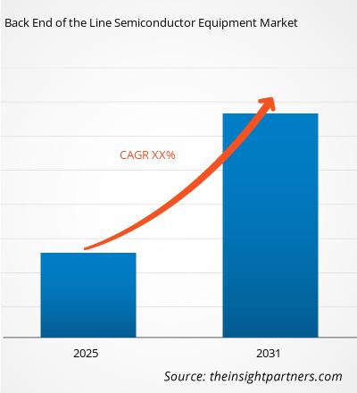
The Back End of the Line Semiconductor Equipment Market Size was valued at US$ 8.22 Billion in 2025 and is projected to reach US$ 18.82 Billion by 2034, growing at a CAGR of 9.64% from 2026 to 2034. These include the miniaturization of devices, increasing number of interconnects, heterogeneous integration, and increasing process control requirements for memory, foundry, and IDM companies.
The North American region continues to be technology-intensive, and it is estimated that the Back End of the Line Semiconductor Equipment Market size will increase by 8.3%–9.3% during the period from 2026 to 2034. The reasons behind the growth include the increased fabrication capacity due to the CHIPS Act, pilot lines for advanced packaging, and high capital intensity of logic, memory, and compound semiconductor manufacturing.
Back End of the Line Semiconductor Equipment Market Assessment and Insights
- North America held 14%–18% of the Back End of the Line Semiconductor Equipment Market share in 2025 and is expected to grow at a CAGR between 8.3%–9.3% during 2026–2034, supported by U.S. fab incentives, advanced logic investment, and domestic packaging programs.
- US represented 82%–87% of North America in 2025 and is projected to grow at a CAGR between 8.4%–9.4% during 2026–2034.
- Europe accounted for 8%–12% share in 2025 and is forecast to grow at a CAGR between 7.6%–8.6% during 2026–2034, led by Germany, France, Italy, and the Netherlands.
- Asia Pacific held 66%–70% share in 2025 and is projected to grow at a CAGR between 10.2%–11.2% during 2026–2034, supported by Taiwan, South Korea, China, Japan, and Singapore.
- Largest Segment CVD held a market share of 22%–26% in 2025, with CAGR range of 9.1%–10.1% between 2026–2034.
- High Growth Segment CMP held a market share of 14%–18% in 2025, with CAGR range of 10.6%–11.6% between 2026–2034.
- Key companies analyzed in detail: Applied Materials, Inc., ASML Holding N.V., Canon Inc., SCREEN Holdings Co., Ltd., Hitachi High-Tech Corporation, Coherent Corp., KLA Corporation, Lam Research Corporation, Newtrax Technologies Inc., Nikon Corporation, and Tokyo Electron Limited.
Source: The Insight Partners' analysis based on proprietary research, government publications, company annual reports, investor presentations, industry databases, and expert interviews.
Demand on process equipment has changed from the planar scaling of devices to controlling multi-layer interconnects, integrating low-k dielectrics, copper and cobalt metallization, and wafer uniformity. The Back End of the Line Semiconductor Equipment Market has evolved as well since the control of interconnects is equally important as the creation of transistors at this point.
The future investment will be driven by AI accelerators, high bandwidth memory, chiplets, and regional semiconductor sovereignty initiatives. The Asia Pacific will continue to be the scale engine, while North America and Europe will also start adding capacity for strategic reasons. According to SEMI, global equipment billings in 2025 reached a record of US$135.1 billion, and the recovery of back-end related assembly, packaging, and test demonstrates increased process complexity across the semiconductor supply chain.
Back End of the Line Semiconductor Equipment Market Report Scope
| Report Attribute | Details |
|---|---|
| Market size in 2025 | US$ 8.22 Billion |
| Market Size by 2034 | US$ 18.82 Billion |
| Global CAGR (2026 - 2034) | 9.64% |
| Historical Data | 2021-2024 |
| Forecast period | 2026-2034 |
Back End of the Line Semiconductor Equipment Market Analysis
There is increasing demand due to the greater number of interconnect layers, tighter control on dielectric thicknesses, and defectivity on the wafer surface associated with more advanced nodes. The Back End of the Line Semiconductor Equipment Market Forecast is supported by AI servers, HBM stacks, and logic devices requiring low-resistance connections and maintaining critical dimension uniformity post-transistor manufacturing.
The supply chain consists of materials providers, chamber sub-system providers, metrology providers, process equipment providers, fab automation providers, and semiconductor manufacturers. Platform competitiveness favors systems with high availability, contamination control, and recipe flexibility. Lead time sensitivities include specialty parts, vacuum sub-systems, power electronics, and customer qualification cycles.
The competitive landscape is dominated by general process equipment providers as well as dedicated lithography, coating, cleaning, metrology, and etch vendors. Applied Materials, Inc., Lam Research Corporation, Tokyo Electron Limited, SCREEN Holdings Co., Ltd., KLA Corporation, and Hitachi High-Tech Corporation compete in terms of process portfolio strength, scale of services, and depth of installed base. Back End of the Line Semiconductor Equipment Market Report now places greater emphasis on the integration of the ecosystem rather than sheer number of tools sold.
Investment trends are shifting towards selective etch technologies, low-temperature deposition, advanced CMP consumables management, and better wet cleaning of copper, dielectric, and barrier films. ASML Holding N.V., Canon Inc., Nikon Corporation, Coherent Corp., and Newtrax Technologies Inc. assist with lithography, optics, process diagnostics, and digitalization solutions to enable fabs improve yield and equipment efficiency.
● REPORT CUSTOMIZATION
Tailor This Report To Align With Your Specific Business Requirements
This report can be customized to align precisely with your business objectives, scope, and target markets. Customization options include tailored segmentation, geography, competitive analysis, and strategic insights to support informed decision-making.
Customize This Report →WHAT YOU CAN ADJUST
- ● Segmentations
- ● Geography
- ● Competitive Analysis
- ● Language Preferences
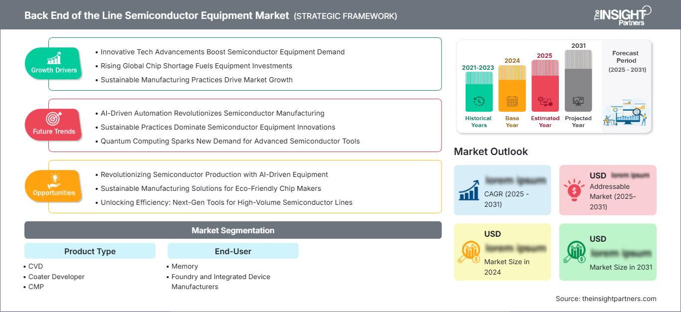
Back End of the Line Semiconductor Equipment Market: Strategic Insights
Regional Insights
North America Back End of the Line Semiconductor Equipment Market
North America held 14%–18% share in 2025 and is expected to expand at 8.3%–9.3% through 2034. The Back End of the Line Semiconductor Equipment Market share is supported by U.S. fabrication incentives, advanced packaging pilots, and reshoring of strategic semiconductor capacity. Logic, memory, and specialty fabs require deposition, etch, wet process, and CMP tools that support high-yield interconnect formation.
Regional procurement is influenced by tool qualification at leading-edge and mature-node fabs, where downtime can constrain wafer starts. Applied Materials, Inc., Lam Research Corporation, KLA Corporation, and Coherent Corp. maintain strong customer engagement through process engineering, service networks, and installed base support. Demand is strongest where government-backed fabs align with AI, defense, automotive, and high-performance computing priorities.
U.S. Back End of the Line Semiconductor Equipment Market Market
The U.S. represented 82%–87% of North American demand in 2025 and is projected to grow at 8.4%–9.4%. Domestic fabs are expanding logic, memory, and specialty capacity, creating demand for CVD, PVD, etch, wet station, and CMP platforms. Semiconductor policy, defense electronics, and cloud infrastructure requirements create a durable base for local equipment support.
Company presence is strengthened by U.S.-based process tool leaders and customer engineering teams serving advanced fabs. Applied Materials, Inc., Lam Research Corporation, KLA Corporation, and Coherent Corp. support deposition, etch, inspection, materials, and optics requirements. Application trends include copper interconnect scaling, HBM support, chiplet packaging interfaces, and factory automation that improves tool utilization.
Europe Back End of the Line Semiconductor Equipment Market Market
Europe accounted for 8%–12% share in 2025 and is expected to grow at 7.6%–8.6%. Germany leads through automotive electronics, power semiconductor manufacturing, and equipment engineering depth. France adds strategic fabrication and research capacity, while Italy and Spain support industrial and power device supply chains. The Netherlands remains critical through lithography and semiconductor ecosystem concentration.
European demand is shaped by energy-efficient chips, automotive reliability standards, and regional sovereignty objectives. ASML Holding N.V., ASML-adjacent suppliers, Tokyo Electron Limited, SCREEN Holdings Co., Ltd., and KLA Corporation serve fabs requiring lithography alignment, wet cleaning, inspection, and process control. Growth is moderate compared with Asia Pacific because fab additions are selective and often focused on specialty technologies.
APAC Back End of the Line Semiconductor Equipment Market Market
APAC held 66%–70% share in 2025 and is projected to grow at 10.2%–11.2%. Taiwan leads advanced foundry demand, South Korea drives HBM and DRAM investment, China sustains mature-node and selective advanced capacity, and Japan supports materials, tools, and specialty fabs.
Industrial policy, local equipment ecosystems, and high wafer starts reinforce regional dominance. Tokyo Electron Limited, SCREEN Holdings Co., Ltd., Hitachi High-Tech Corporation, Canon Inc., Nikon Corporation, and Lam Research Corporation support deposition, cleaning, lithography, etch, and process control. India, Singapore, and Australia add incremental demand through packaging, research, and supply-chain diversification initiatives.
Middle East & Africa Back End of the Line Semiconductor Equipment Market Market
Middle East & Africa is projected to grow at 5.8%–6.8%, with Saudi Arabia and the UAE exploring semiconductor-linked diversification, data center infrastructure, and electronics localization. South Africa remains the most established electronics base, while Rest of MEA demand is concentrated in research, training, and limited specialty manufacturing.
Energy revenue, sovereign wealth investment, and digital infrastructure programs support early-stage semiconductor ecosystem building. However, limited high-volume wafer fabrication, talent constraints, and import dependence keep regional equipment demand below global hubs. Opportunities are strongest in pilot lines, packaging services, university labs, and industrial electronics projects requiring controlled deposition, cleaning, and inspection capability.
Segmentation Analysis
Product Type
Product Type is projected to grow at 9.2%–10.2% during 2026–2034. Back End of the Line Semiconductor Equipment Market trends covers deposition, patterning support, planarization, etching, wet cleaning, and stepper systems used after transistor formation. Adoption depends on interconnect complexity, yield targets, wafer size, process node maturity, and fab-specific integration requirements.
- CVD remains the largest product category because dielectric, barrier, and passivation layer deposition is essential for interconnect reliability, device isolation, and multilayer routing across logic and memory fabs.
- Coater Developer systems support lithography preparation and post-exposure processing, making them strategically important wherever tighter overlay, uniform resist films, and repeatable pattern transfer determine yield.
- CMP demand is rising as multilayer interconnect stacks require precise planarization, lower defectivity, and improved surface control before subsequent deposition, etch, and lithography steps.
- Metal Etching tools address copper, aluminum, and barrier layer patterning requirements, where selectivity, profile control, and residue management directly influence device performance and electrical reliability.
- PVD platforms are used for metal seed, barrier, and adhesion layers, supporting interconnect formation where film uniformity, step coverage, and contamination control affect downstream yield.
- Wet Station equipment supports cleaning, stripping, and surface preparation, remaining critical as fabs manage particles, residues, and chemical compatibility across increasingly complex wafer process flows.
- Stepper systems serve patterning requirements in mature and selected back-end layers, particularly where cost-efficient lithography, alignment accuracy, and high throughput remain more important than leading-edge EUV capability.
End-User
End-User is forecast to grow at 9.5%–10.5% during 2026–2034. Memory manufacturers lead advanced planarization and deposition requirements, foundries drive process breadth across nodes and customers, and integrated device manufacturers maintain demand for controlled, long-life equipment in logic, analog, power, and specialty semiconductor production.
- Memory demand is driven by DRAM, NAND, and HBM architectures that require dense interconnects, uniform films, reliable CMP, and defect control to support bandwidth, capacity, and endurance targets.
- Foundry users require flexible equipment platforms across customer designs, process nodes, and packaging interfaces, making uptime, recipe portability, and process control central to purchasing decisions.
- Integrated Device Manufacturers invest in durable tools for captive production where power, analog, logic, and specialty devices need stable yields, long process lifecycles, and controlled ownership costs.
Opportunity Snapshot
| End-User | Revenue Contribution | Trend Tag | Adoption Stage |
| Memory | High | HBM Expansion | Scaling |
| Foundry | High | Advanced Logic | Mature-to-Advanced |
| Integrated Device Manufacturers | Medium | Specialty Nodes | Mature |
Back End of the Line Semiconductor Equipment Market Growth Drivers and Impact Analysis
AI and HBM Increase Interconnect Process Intensity
AI accelerators and high-bandwidth memory parts enhance the importance of interconnect control due to the influence of resistance, layer uniformity, and defects on the speed and power efficiency. Along with the scaling of HBM stacks and advanced logic, the fabs become more demanding regarding the deposition, etching, CMP, and wet clean control. The data from SEMI indicates that the test equipment billings increased in 2025 together with assembly and packaging equipment, meaning additional complexity beyond transistors. Practically speaking, it implies more costs for each wafer start, longer qualifying processes, and more interest in vendors who are capable of integrating process know-how with yield knowledge.
Regional Fab Incentives Reshape Equipment Localization
Semiconductor sovereignty initiatives from the United States, Europe, Japan, South Korea, Taiwan, and China will transform equipment purchasing through regional fabs, local field service operations, and resiliency in the supply chain. The effect is clear in the increased requirement for installation, maintenance, spares, and process engineering closer to the end customer. It becomes challenging to coordinate export controls, customer-specific configurations, and regional procurement needs while ensuring manufacturing efficiencies on a global scale. In such conditions, companies with a balanced manufacturing presence around the globe along with robust field service capabilities and advanced and mature node customers will prosper.
Yield Pressure Drives Process Control Investment
End-of-line defects may impair device performance even if the front-end transistor features satisfy specification requirements. With shrinking and increasing layers of interconnects, yield loss due to particles, residues, dishing, erosion, and film uniformity is greater. Consequently, fabs are now making efforts to acquire systems which combine cleaner chemistries, reliable endpoint detection, chamber matching, and in-process control. This will have a market effect in the form of moving from purchase decisions for equipment based on pure throughput to those made to safeguard yield and cost of ownership. The companies benefiting from such an environment include KLA Corporation, Hitachi High-Tech Corporation, and process tool manufacturers.
Back End of the Line Semiconductor Equipment Market Future Trends
Selective Deposition and Low-Damage Etch Move Mainstream
Back End of the Line Semiconductor Equipment Market trends will move towards selective deposition, low-damage etching and process sequences that will lower integration steps as well as provide protection for low-k dielectrics. In cases when interconnect geometries get smaller and blanket deposition and subtractive patterning is used, there can be residues left behind, sidewall damage or resistance variation. Selective deposition will make it possible to put down materials where they are required without causing CMP steps and susceptibility to defects. It will be dependent upon the ability of suppliers to show improvement in yields across several device structures to become standard practice.
Equipment Intelligence Becomes a Yield Differentiator
It is anticipated that process tools will evolve to be more data-centric as fabs link sensor data streams, chamber history, wafer maps, and metrology data with their predictive control systems. Back-end processes are particularly amenable to this development because minor fluctuations in polishing, cleaning, or etching could lead to electrical performance problems. The equipment’s intelligence will enable quick recipe adjustment, early detection of faults, and better matching among tool fleets. Data security, customer confidence, and compatibility of tool vendors and fab automation systems will be needed for adoption. This development will favor vendors who have both reliable hardware and analytics/software capabilities.
Back End of the Line Semiconductor Equipment Market Opportunities
HBM-Centric Memory Capacity Expansion
An investment opportunity clearly exists in the memory market due to increased needs for high quality interconnects, planarized surface, and wafer-level uniformity prior to advanced packaging driven by HBM development. BEOL Semiconductor Equipment Market Forecast indicates tool upgrade opportunities in CVD, CMP, PVD, and wet cleaning to achieve higher throughput without compromising yields in memory fabs. Investments in process modules which alleviate film stress, improve dielectric performance, and copper line stabilization are also possible. This is especially true in South Korea, Taiwan, Japan, and China where memories and foundries tend to be localized near material/component suppliers. Collaboration with memory leaders could develop replicable processes for future generations of HBM.
Service-Led Upgrades for Mature-Node Fabs
The reason why mature node fabs continue to be commercially viable is that there are applications in the form of automotive, industrial, power management, sensing, and connectivity that rely on stable process flow. The approach that most customers would take is not the replacement of the whole line, but rather an upgrade to chambers, controls, wet stations, and CMP process. There is money for vendors to make through extending the lifespan of their tools, increasing availability, and decreasing consumables variance. The appeal of this business model lies in the fact that mature node fabs tend to operate under long-lived product cycles and prefer reliability to being cutting-edge.
Recent Developments
- June 2026: Applied Materials, Inc. introduced new systems to accelerate DRAM and advanced packaging for AI chips, strengthening its deposition, materials engineering, and integration roadmap for memory and heterogeneous architectures. The launch supports customer requirements for higher bandwidth, improved interconnect performance, and scaling efficiency in AI-driven semiconductor production.
- May 2026: Applied Materials, Inc. and SCREEN Holdings Co., Ltd. announced a partnership to bring advanced wafer cleaning technologies to the EPIC Center, focusing on co-optimization of process steps for next-generation semiconductor manufacturing. The collaboration aligns wet cleaning expertise with materials engineering needs in advanced interconnect and packaging flows.
- December 2025: Rigaku Corporation, a global solution partner in X-ray analytical systems and a group company of Rigaku Holdings Corporation (headquarters: Akishima, Tokyo; CEO: Jun Kawakami; hereinafter “Rigaku”) announced the launch of the ONYX 3200, a new semiconductor metrology system to measure film thickness, composition and bump* structures for wafer-level processes. The system is engineered to help manufacturers stabilize quality and increase yield in the metal-wiring formation (back-end-of-line (BEOL)) and packaging processes of semiconductor chips.
Frequently Asked Questions

- Comprehensive Market Sizing and Forecast Analysis
- Detailed Segmentation Analysis
- In-Depth Market Dynamics Assessment
- Regional and Country-Level Insights
- Competitive Landscape and Company Benchmarking
- Strategic Business Intelligence
Recent Reports
Testimonials

The Insight Partners' SCADA System Market report is comprehensive, with valuable insights on current trends and future forecasts. The team was highly professional, responsive, and supportive throughout. We are very satisfied and highly recommend their services.
RAN KEDEM Partner, Reali Technologies LTDs
I requested a report on a very specific software market and the team produced the report in a few days. The information was very relevant and well presented. I then requested some changes and additions to the report. The team was again very responsive and I got the final report in less than a week.
JEAN-HERVE JENN Chairman, Future Analytica
We worked with The Insight Partners for an important market study and forecast. They gave us clear insights into opportunities and risks, which helped shape our plans. Their research was easy to use and based on solid data. It helped us make smart, confident decisions. We highly recommend them.
PIYUSH NAGPAL Sr. Vice President, High Beam Global
The Insight Partners delivered insightful, well-structured market research with strong domain expertise. Their team was professional and responsive throughout. The user-friendly website made accessing industry reports seamless. We highly recommend them for reliable, high-quality research services
YUKIHIKO ADACHI CEO, Deep Blue, LLC.
This is the first time I have purchased a market report from The Insight Partners.While I was unsure at first, I visited their web site and felt more comfortable to take the risk and purchase a market report.I am completely satisfied with the quality of the report and customer service. I had several questions and comments with the initial report, but after a couple of dialogs over email with their analyst I believe I have a report that I can use as input to our strategic planning process.Thank you so much for taking the extra time and making this a positive experience.I will definitely recommend your service to others and you will be my first call when we need further market data.
JOHN SUZUKI President and Chief Executive Officer, Board Director, BK Technologies
I wish to appreciate your support and the professionalism you displayed in the course of attending to my request for information regarding to infectious disease IVD market in Nigeria. I appreciate your patience, your guidance, and the fact that you were willing to offer a discount, which eventually made it possible for us to close a deal. I look forward to engaging The Insight Partners in the future, all thanks to the impression you have created in me as a result of this first encounter.
DR CHIJIOKE ONYIA MANAGING DIRECTOR, PineCrest Healthcare Ltd.Reason to Buy
- Informed Decision-Making
- Understanding Market Dynamics
- Competitive Analysis
- Identifying Emerging Markets
- Customer Insights
- Market Forecasts
- Risk Mitigation
- Boosting Operational Efficiency
- Strategic Planning
- Investment Justification
- Tracking Industry Innovations
- Aligning with Regulatory Trends





 Get Free Sample for