
Dicing Tapes Market Growth, Trends & Demand by 2034
Coverage: By Product (UV Curable Dicing Type, Non-UV Curable Dicing Type); Backing Material (Polyvinyl Chloride , PET , Polyolefin , Others); Coating (Single Sided , Double Sided) , and Geography (North America, Europe, Asia Pacific, and South and Central America)
- Status : Data Released
- Report Code : TIPRE00022545
- Category : Chemicals and Materials
- No. of Pages : 150
- Available Report Formats :


- Last update date : July 20, 2026


2025 Market Size
US$ 1.49 Bn
Base year value
2034 Forecast
US$ 2.50 Bn
Projected by 2034
CAGR 2026-2034
5.89 %
Growth rate
Addressable Market
US$ 18.05 Bn
(2026-2034)
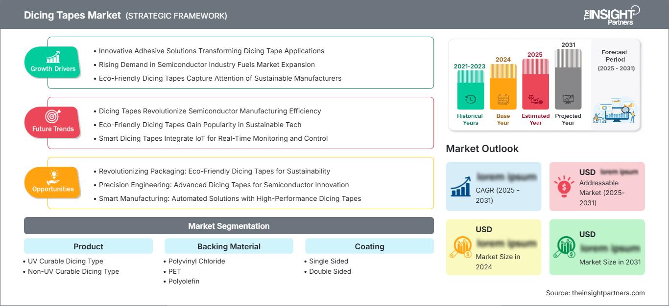
The Dicing Tapes Market size was US$ 1.49 Billion in 2025 and is estimated to be US$ 2.50 Billion by 2034, growing at a CAGR of 5.89% from 2026 to 2034. The growing demand for wafer thinning in semiconductor wafer processing, advanced packaging applications, clean picking up of dies, and singulation are factors driving the market.
North America is one of the technically advanced regions of the world, where the expected market growth rate will be between 4.8-5.6%. The growing demand from fabs, OSATs, and specialty semiconductor device manufacturers is the factor behind growing demand for high-quality UV release films. There is significant demand from automotive electronics, MEMS, photonics, and military-grade semiconductors.
Dicing Tapes Market Assessment and Insights
- North America: Share in 2025 of 21–25% and CAGR between 4.8–5.6%. Demand is led by advanced packaging pilots, MEMS, automotive electronics, and localized semiconductor supply-chain investment.
- US: Share in 2025 of 82–86% of North America and CAGR between 4.9–5.7%. Domestic fabs, defense electronics, photonics, and OSAT investments sustain adoption of premium UV-release tapes.
- Europe: Share in 2025 of 15–19% and CAGR between 4.3–5.1%. Germany, France, Italy, the UK, and Spain contribute demand through power semiconductors, automotive electronics, sensors, and microelectronics programs.
- Asia Pacific: Share in 2025 of 52–56% and CAGR between 6.3–7.1%. China, Japan, South Korea, Taiwan, India, and Southeast Asia lead volume consumption due to concentrated wafer fabrication and packaging capacity.
- Largest Segment: UV Curable Dicing Type held market share of 56–60% in 2025 and CAGR of 6.1–6.9% during 2026–2034, supported by controlled release in thin-wafer processing.
- High Growth Segment: Polyolefin backing material held market share of 24–28% in 2025 and CAGR of 6.8–7.6% during 2026–2034, driven by flexibility, cleanliness, and advanced package compatibility.
- Key companies analyzed in detail: Nitto Denko Corporation, LINTEC Corporation, Sumitomo Bakelite Co., Ltd., Denka Company Limited, Furukawa Electric Co., Ltd., 3M Company, Mitsui Chemicals, Inc., Resonac Corporation, Pantech Tape Co., Ltd., Ultron Systems, Inc.
Source: The Insight Partners' analysis based on proprietary research, government publications, company annual reports, investor presentations, industry databases, and expert interviews.
The evolution of the market has driven dicing tapes from simple holding films to more sophisticated process films affecting wafer yield and die performance. The new generation of UV-curable acrylic adhesives, cleaner PVC, PET, and polyolefin films, and antistatic coatings can now handle extremely thin wafers, compound semiconductors, and small dies. Suppliers are also refining coating uniformity, particle reduction, and post-UV peelability to allow high-speed dicing, laser singulation, and automated pick-and-place applications.
The demand for future growth will be stronger in regions investing in semiconductor manufacturing capacity, including Asia Pacific and US. Favorable public policies for local chip manufacturing, increasing contamination requirements, and rising investments in AI, EVs, 5G, and industrial electronics have raised the need for process tapes. Those tape suppliers who offer cleanroom coating, application engineering, and qualification assistance can benefit from the long-cycle customer approval process.
Dicing Tapes Market Report Scope
| Report Attribute | Details |
|---|---|
| Market size in 2025 | US$ 1.49 Billion |
| Market Size by 2034 | US$ 2.50 Billion |
| Global CAGR (2026 - 2034) | 5.89% |
| Historical Data | 2021-2024 |
| Forecast period | 2026-2034 |
Dicing Tapes Market Analysis
Dicing Tapes Market growth is associated with semiconductors unit production volume, wafer thinning, die scaling down, and heterogeneous integration. With chip architectures moving towards stacked memories, chiplets, MEMS, power modules, and compound semiconductor products, dicing process becomes critical for yield. The tape should be able to securely fix wafer during cutting either by mechanical sawing or laser process, releasing dies without any edge damage, contamination, and ESD.
The value chain consists of base film manufacturers, adhesive manufacturers, coating technologies providers, wafer handling equipment makers, fabs, and OSATs. UV-curable tapes will lower picking up force post exposure, but in some cases, non-UV tapes are preferred due to lower costs, standard wafer thickness, and simplicity of technology. Favorable supply environment promotes Japanese and American companies with qualification record, however, local sourcing trends promote selected Asian suppliers to increase capacities and engineering support.
Current Dicing Tapes Market dynamics are based on cleanroom manufacturing control, chemistry of adhesive, and customer qualification process rather than pricing alone. Nitto Denko Corporation, LINTEC Corporation, Sumitomo Bakelite Co., Ltd., and Furukawa Electric Co., Ltd. are key players in the market due to comprehensive portfolio of semiconductors processing tapes and technical assistance in handling thin wafers, package dicing, and compound semiconductor substrates.
Denka Company Limited, 3M Company, Mitsui Chemicals, Inc., Resonac Corporation, Pantech Tape Co., Ltd., and Ultron Systems, Inc. add value to the competition via coating technology, wafer mounting solutions, specialized adhesives, and regional customer relations. Competitive positioning becomes increasingly associated with advanced packaging development plans, antistatic features, contamination control and qualification tests across various types of wafers.
● REPORT CUSTOMIZATION
Tailor This Report To Align With Your Specific Business Requirements
This report can be customized to align precisely with your business objectives, scope, and target markets. Customization options include tailored segmentation, geography, competitive analysis, and strategic insights to support informed decision-making.
Customize This Report →WHAT YOU CAN ADJUST
- ● Segmentations
- ● Geography
- ● Competitive Analysis
- ● Language Preferences
Dicing Tapes Market: Strategic Insights
Regional Insights
North America Dicing Tapes Market
North America accounted for 21–25% of global revenue in 2025 and is projected to grow at a 4.8–5.6% CAGR during 2026–2034. The region benefits from fab expansion incentives, advanced packaging research, defense electronics programs, and strong demand for high-reliability process materials. The Dicing Tapes Market share is supported by US wafer capacity and specialized device production.
Local buyers stress compatibility with the cleanroom environment, low ionic contamination, and a proven track record in thin-wafer processes. Automotive electronics, MEMS, RF components, photonic chips, and silicon carbide packaging are demanding higher standards for adhesion stability and die release. Well-developed distribution channels and local application engineering groups assist suppliers with faster evaluations despite most consumables being tied to Asian production capacity.
U.S. Dicing Tapes Market
The U.S. accounted for 82–86% of North American sales in 2025 and should grow with a 4.9–5.7% CAGR during 2034. Demand is driven by new fabs, R&D pilot lines, compound semiconductors, and military electronics fabrication. The application area shows growing preference towards UV release tapes for thinned silicon, MEMS, photonics, and high-end specialty wafers.
Company presence is indicated through products and services rather than the presence of coating facilities domestically. Both 3M Company and Ultron Systems, Inc. serve the local customer base, whereas Japanese suppliers have strong qualification at multinational semiconductor manufacturers. Demand will continue to be concentrated in applications where process reliability, traceability, and supplier responsiveness prevail over inexpensive tape procurement.
Europe Dicing Tapes Market
Europe accounted for 15-19% of the global revenue share in 2025 and is expected to register a CAGR of 4.3-5.1% between 2026 and 2034. Germany is the largest country due to its automotive semiconductor, power electronics, sensors, and industrial automation sectors. The UK adds demand through its compound semiconductor research and photonics technologies, while Germany’s wafer/module ecosystem generates demand for qualified tapes.
France gains from microelectronic clusters and government support for chip manufacturing capacity, whereas Italy and Spain generate demand due to their power devices, electronics assembly, and automotive industries. Users are concerned about environment-related issues, process control, and availability of quality material imports. Supplier differentiation is determined by the capability to fulfill the requirement of low residue, antistatic, and heat resistance properties.
APAC Dicing Tapes Market
The Asia Pacific region represented 52-56% of global revenues in 2025, and is expected to grow at a CAGR of 6.3-7.1%. China, Japan, South Korea, Taiwan, India, and Australia are engaged via the wafer fabrication, OSAT, electronics assembly, and specialty devices. Japan is the foremost provider base for premium grade tapes, whereas China and Southeast Asia provide for volume growth.
Industries that serve as important anchors for demand include industrial policy, AI hardware, smartphone supply chain, electric vehicles, and memory manufacturing. The tape is needed in South Korea and Taiwan due to its high-performance requirements for advanced packaging and memory processes. India's semiconductor policy serves as an anchor for the beginning of material demand.
Middle East & Africa Dicing Tapes Market
The Middle East & Africa region is expected to register a 4.7–5.5% CAGR through 2034. Saudi Arabia, the UAE, South Africa, and the rest of MEA remain smaller demand centers, but electronics assembly, research infrastructure, and diversification programs are improving long-term prospects. Energy transition projects also increase demand for power electronics and sensors.
The UAE leads in regional adoption through its investments in technology, logistics, and electronics distribution networks. Saudi Arabia is investing in industrial diversification and advanced manufacturing, while South Africa is promoting niche electronics and auto parts supply chain development. The growth depends on wafer-processing consumable imports, regional packaging collaborations, and the development of semiconductor-related competencies.
Segmentation Analysis
Product
The Product segment is projected to grow at a 5.7–6.5% CAGR during 2026–2034. The Dicing Tapes Market scope is shaped by the balance between high-adhesion wafer holding and clean die release. UV curable products dominate advanced processes, while non-UV tapes remain suitable for conventional wafers, lower-cost packaging, and less complex singulation flows.
- UV Curable Dicing Type: This type leads advanced wafer processing because adhesion drops after ultraviolet exposure, enabling cleaner pick-up for thin wafers, small dies, MEMS, and high-density semiconductor packages.
- Non-UV Curable Dicing Type: Non-UV products retain demand in standard wafer processing where cost control, simple equipment flows, and stable mechanical holding are more important than controlled post-exposure release.
Backing Material
The Backing Material segment is expected to register a 5.9–6.7% CAGR through 2034. Material selection affects stretch behavior, conformability, particle generation, wafer support, and compatibility with automated mounting tools. PVC remains widely used, PET supports dimensional stability, and polyolefin is gaining traction where flexibility, low contamination, and package-level dicing performance are critical.
- Polyvinyl Chloride: PVC films remain common due to balanced cost, adhesion support, flexibility, and established qualification in silicon wafer dicing, especially for standard product families.
- PET: PET backing provides dimensional stability and clean processing characteristics for applications requiring consistent film behavior, accurate wafer support, and reliable handling during automated mounting.
- Polyolefin: Polyolefin films are increasingly preferred for advanced packages and thin wafers because they combine flexibility, cleanliness, and controlled mechanical behavior under demanding singulation conditions.
Coating
The Coating segment is forecast to expand at a 5.5–6.3% CAGR during 2026–2034. Coating architecture determines adhesion uniformity, residue control, surface cleanliness, and handling reliability. Single-sided tapes dominate wafer dicing, while double-sided formats serve specialized transfer, temporary bonding, and process support applications where secure attachment on both surfaces improves workflow control.
- Single Sided: Single-sided tapes are the primary choice for wafer mounting because they provide controlled adhesion to the wafer backside while maintaining compatibility with frames and automated handling equipment.
- Double Sided: Double-sided tapes serve specialized semiconductor support tasks where temporary bonding, transfer stability, or fixture attachment is needed during package-level processing and precision assembly.
Opportunity Snapshot
| Segment Name | Revenue Contribution | Trend Tag | Adoption Stage |
| UV Curable Dicing Type | High | Thin Wafers | Mature |
| Non-UV Curable Dicing Type | Medium | Standard Dicing | Mature |
Dicing Tapes Market Growth Drivers and Impact Analysis
Advanced Packaging and Wafer Thinning Requirements
The use of advanced packaging technology is driving up the process value of dicing tapes since ultra-thin wafers, chiplets, stacked memory, and compound semiconductor substrates are susceptible to breaking, cracking, and contamination. With thinning of the wafers and reducing die sizes, the adhesive materials have to be stronger for temporary bonding and release in the pick-up stage. The UV curable dicing tapes offer reduction in mechanical stresses during curing, ensuring higher yields with high-valued products. This is having a direct market effect on the dicing tapes since the tapes will go through a process qualification within the packaging reliability process and not just purchased as consumables.
Growth in Automotive, AI, and Power Electronics Devices
Demand for semiconductors used in electric vehicles, artificial intelligence servers, data centers, industrial automation, and renewable energy systems will fuel an increase in wafer starts for logic, memory, sensor, and power devices. This will translate into an increased need for tapes that can provide better process window capability for the reliable singulation of silicon, silicon carbide, gallium nitride, and substrate packages. It is particularly important to note that automotive qualification is critical, as the supplier must meet stricter requirements for reliability, traceability, and contamination control. The effect on the market will be seen through the growing use of premium tapes, longer qualification periods, and higher technical support needs.
Rising Cleanliness and Yield-Control Standards
Yield control is becoming a decisive purchasing factor as semiconductor manufacturers process higher-value wafers and more complex packages. Particle contamination, adhesive transfer, unstable peel force, and wafer deformation can generate costly defects during dicing and die attach. As a result, customers increasingly demand tapes made in controlled environments with consistent coating thickness, low outgassing, and documented material properties. This driver shifts competition toward quality systems and process knowledge. Suppliers that can support audits, failure analysis, and application-specific recommendations strengthen customer trust. The impact is strongest in advanced nodes, MEMS, photonics, and power devices, where consumables quality can influence equipment uptime, die loss, and downstream package reliability.
Dicing Tapes Market Future Trends
Process-Specific UV Release and Antistatic Formulations
Future Dicing Tapes Market trends will center on formulations tailored to wafer material, die size, and singulation method. UV-release adhesives are expected to become more process-specific, with controlled peel-force reduction, lower residue, and improved compatibility with laser dicing, plasma dicing, and ultra-thin wafers. Antistatic designs will gain importance as AI, memory, and sensor devices become more sensitive to electrostatic discharge. Suppliers may increasingly offer application matrices rather than broad general-purpose tapes, helping customers reduce trial time and improve yield. This trend will favor companies with deep coating chemistry, cleanroom manufacturing, and technical teams able to support device-specific qualification programs.
Localized Supply Chains and Qualification Partnerships
Semiconductor supply-chain regionalization will influence how dicing tape suppliers invest in service, inventory, and qualification partnerships. As the United States, Europe, India, Japan, South Korea, and China support domestic chip ecosystems, buyers will expect shorter lead times and stronger local technical support. Tape makers may respond through regional warehousing, joint evaluations with equipment vendors, and closer collaboration with OSATs. The trend will not fully replace established Asian production networks, but it will raise the value of traceability, customer proximity, and rapid troubleshooting. Suppliers that combine global quality standards with local responsiveness should gain preference in new fabs and pilot lines.
Dicing Tapes Market Opportunities
Advanced Packaging Qualification Programs
Advanced packaging qualification offers a high-value opportunity because customers need tapes proven under thin-wafer handling, small-die pick-up, and stacked package conditions. Investment aligned with Dicing Tapes Market Forecasts should prioritize technical laboratories, wafer-level testing support, and co-development with dicing equipment suppliers. Suppliers can differentiate by providing data on post-UV adhesion loss, residue, contamination, tensile behavior, and electrostatic performance. The opportunity is especially attractive in AI accelerators, high-bandwidth memory, automotive power modules, and compound semiconductors. Companies that enter qualification early can secure long product lifecycles, reduce switching risk for customers, and create recurring revenue tied to high-volume packaging platforms.
Polyolefin and Low-Contamination Film Expansion
Polyolefin and low-contamination film expansion presents a practical opportunity for suppliers targeting advanced and specialty devices. As customers process thinner wafers and more fragile substrates, backing films must provide flexibility, mechanical support, and clean release without generating particles or deformation. Investment in improved film extrusion, precision coating, and clean packaging can create measurable process benefits. Suppliers may also develop differentiated grades for silicon carbide, gallium nitride, MEMS, optoelectronics, and package dicing. This opportunity rewards companies that can combine material science with application knowledge, because buyers increasingly evaluate tapes through yield performance, equipment compatibility, and post-dicing defect reduction rather than basic unit price.
Recent Developments
- Feburay 2026: Ahlstrom has launched Acti-V RRF Natural, a sustainable release liner for double-sided Pressure Sensitive Adhesive (PSA) tapes. This innovative product boasts a recyclability rating of Recyclable with Paper1 and uses recycled, unbleached fibers. Its new repulpable formulation allows recyclability even when silicone-coated on both sides. Traditionally, high-density silicone-coated release liners have been difficult to recycle due to their hydrophobic surfaces and high reject rates, earning a Not Recyclable rating in testing.
- January 2026: UltraTape has launched a new Silicone-Free Cleanroom Tape and Label Series, designed to prevent silicone contamination in high-performance environments such as semiconductor, aerospace/defense, medical/pharmaceutical, and advanced electronics manufacturing. Silicone contamination poses significant risks, including adhesion failures and reduced device yield, which can lead to costly rework or product loss.
Frequently Asked Questions

- Comprehensive Market Sizing and Forecast Analysis
- Detailed Segmentation Analysis
- In-Depth Market Dynamics Assessment
- Regional and Country-Level Insights
- Competitive Landscape and Company Benchmarking
- Strategic Business Intelligence
Recent Reports
Testimonials

The Insight Partners' SCADA System Market report is comprehensive, with valuable insights on current trends and future forecasts. The team was highly professional, responsive, and supportive throughout. We are very satisfied and highly recommend their services.
RAN KEDEM Partner, Reali Technologies LTDs
I requested a report on a very specific software market and the team produced the report in a few days. The information was very relevant and well presented. I then requested some changes and additions to the report. The team was again very responsive and I got the final report in less than a week.
JEAN-HERVE JENN Chairman, Future Analytica
We worked with The Insight Partners for an important market study and forecast. They gave us clear insights into opportunities and risks, which helped shape our plans. Their research was easy to use and based on solid data. It helped us make smart, confident decisions. We highly recommend them.
PIYUSH NAGPAL Sr. Vice President, High Beam Global
The Insight Partners delivered insightful, well-structured market research with strong domain expertise. Their team was professional and responsive throughout. The user-friendly website made accessing industry reports seamless. We highly recommend them for reliable, high-quality research services
YUKIHIKO ADACHI CEO, Deep Blue, LLC.
This is the first time I have purchased a market report from The Insight Partners.While I was unsure at first, I visited their web site and felt more comfortable to take the risk and purchase a market report.I am completely satisfied with the quality of the report and customer service. I had several questions and comments with the initial report, but after a couple of dialogs over email with their analyst I believe I have a report that I can use as input to our strategic planning process.Thank you so much for taking the extra time and making this a positive experience.I will definitely recommend your service to others and you will be my first call when we need further market data.
JOHN SUZUKI President and Chief Executive Officer, Board Director, BK Technologies
I wish to appreciate your support and the professionalism you displayed in the course of attending to my request for information regarding to infectious disease IVD market in Nigeria. I appreciate your patience, your guidance, and the fact that you were willing to offer a discount, which eventually made it possible for us to close a deal. I look forward to engaging The Insight Partners in the future, all thanks to the impression you have created in me as a result of this first encounter.
DR CHIJIOKE ONYIA MANAGING DIRECTOR, PineCrest Healthcare Ltd.Reason to Buy
- Informed Decision-Making
- Understanding Market Dynamics
- Competitive Analysis
- Identifying Emerging Markets
- Customer Insights
- Market Forecasts
- Risk Mitigation
- Boosting Operational Efficiency
- Strategic Planning
- Investment Justification
- Tracking Industry Innovations
- Aligning with Regulatory Trends





 Get Free Sample for