
GaN-on-Silicon Technology Market Growth, Trends & Demand by 2034
Coverage: by Wafer Size (50 mm, 100 mm, 150 mm, 200 mm); Industry Vertical (Automotive, Aerospace and Defense, Consumer Electronics, IT and Telecom, Others) , and Geography (North America, Europe, Asia Pacific, and South and Central America)
- Status : Data Released
- Report Code : TIPRE00006219
- Category : Electronics and Semiconductor
- No. of Pages : 150
- Available Report Formats :


- Last update date : August 17, 2026


2025 Market Size
US$ 2.18 Bn
Base year value
2034 Forecast
US$ 7.48 Bn
Projected by 2034
CAGR 2026-2034
14.68 %
Growth rate
Addressable Market
US$ 41.40 Bn
(2026-2034)
The Gan-on-Silicon Technology Market was valued at US$ 2.18 Billion in 2025 and is projected to reach US$ 7.48 Billion by 2034, growing at a CAGR of 14.68% from 2026 to 2034. Demand is anchored in wide-bandgap efficiency, lower switching losses, compact thermal design, and silicon-line scalability across automotive, aerospace and defense, consumer electronics, and IT and telecom systems.
Across North America, the Gan-on-Silicon Technology Market size is supported by an estimated 13.8–14.6% CAGR through 2034, reflecting 5G radio modernization, AI data-center power density needs, and domestic compound-semiconductor investment. Growth is reinforced by 200 mm wafer migration, defense electronics demand, EV charging infrastructure, and stricter efficiency expectations for server power supplies and compact consumer adapters.
GaN-on-Silicon Technology Market Assessment and Insights
- North America held 31–33% share in 2025 and is expected to grow at a CAGR of 13.8–14.6% between 2026–2034, led by U.S. semiconductor funding, 5G networks, and AI data-center power upgrades.
- US represented 76–79% of North America in 2025 and is projected to grow at a CAGR of 13.7–14.5% between 2026–2034, supported by domestic wide-bandgap device manufacturing.
- Europe accounted for 22–24% share in 2025 and is forecast to grow at a CAGR of 13.1–13.9% between 2026–2034, with Germany, France, the UK, Italy, and Spain leading adoption.
- Asia Pacific captured 36–39% share in 2025 and is projected to grow at a CAGR of 15.4–16.2% between 2026–2034, led by China, Japan, South Korea, India, and Taiwan-linked electronics supply chains.
- Largest Segment 150 mm wafers held 39–42% market share in 2025 and are expected to grow at a CAGR of 13.2–14.0% between 2026–2034 due to mature production economics.
- High Growth Segment 200 mm wafers held 24–27% market share in 2025 and are projected to expand at a CAGR of 16.0–17.0% between 2026–2034 as fabs pursue cost-per-device reduction.
- Key companies analyzed in detail: Coherent Corp., DS4 Laser Technology GmbH, GAM Laser Inc., Linde plc, MS Technologies AG, PaR Systems LLC, Rofin Laser Micro, Sacher Lasertechnik GmbH, SUSS MicroTec SE, Yokogawa Electric Corporation.
Source: The Insight Partners' analysis based on proprietary research, government publications, company annual reports, investor presentations, industry databases, and expert interviews.
Technology migration has resulted in a transition of the Gan-on-Silicon Technology from specialty RF and discrete power to volume-based power conversion, high-frequency communication, and module integration. Process technology trends are moving towards more compatible processing of silicon wafers, enhanced epitaxial buffer layers, and large-diameter substrates to drive down the die costs, and increase uniformity. Equipment suppliers are responding to changing demands for higher yields, wafer bow control, and more reliability data for entry into the automotive and infrastructure business.
Future market demand will be bolstered by the increased importance of compact semiconductors in data center power densities, EV charging stations, satellite communications, and 5G small cell roll-outs. Geographies with favorable trends include public backing of semiconductor localization and electrification of industry. In addition, the future looks bright due to the energy efficiency mandate, which means less loss and lower operating power for high-volume electronics and RF infrastructure.
GaN-on-Silicon Technology Market Report Scope
| Report Attribute | Details |
|---|---|
| Market size in 2025 | US$ 2.18 Billion |
| Market Size by 2034 | US$ 7.48 Billion |
| Global CAGR (2026 - 2034) | 14.68% |
| Historical Data | 2021-2024 |
| Forecast period | 2026-2034 |
GaN-on-Silicon Technology Market Analysis
The market for GaN-on-silicon Technology is driven by various demand drivers that influence the overall trajectory of its development. Increasing global awareness about energy efficiency and carbon emissions has made GaN-on-silicon the key technology in the development of next-generation power electronics. Electric vehicle makers have started to utilize GaN-based systems for their chargers, DC-DC converters, and traction inverters for power density improvements and decreased charging time. At the same time, the consumer electronics segment keeps introducing GaN technology for compact and highly efficient power adapters and chargers as a response to customer demands for compactness and increased charging speeds. The migration of the telecommunication industry to 5G network infrastructure generated high demand for RF amplifiers with high frequencies and high power, in which GaN-on-silicon performs much better than alternative LDMOS and GaAs solutions.
The competitive environment within the Gan-on-Silicon Technology Market Report is comprised of semiconductor equipment companies, GaN technology firms, and firms that are vertically integrated. Among the firms mentioned above are COHERENT, Suss MicroTec, and Yokogawa, each bringing complementary technology in materials processing equipment, wafer bonding equipment, and testing and measurement solutions, respectively. The use of partnerships and collaborative efforts has become increasingly popular among market participants that attempt to incorporate their technologies in comprehensive products for end users. The growth in the investments in the Market can be seen from the fact that venture capital is being directed towards Gan startups, as well as existing companies that expand their production capacity. The consolidation through acquisitions and partnerships is a trend in the market that allows companies to enhance their technological and market position.
● REPORT CUSTOMIZATION
Tailor This Report To Align With Your Specific Business Requirements
This report can be customized to align precisely with your business objectives, scope, and target markets. Customization options include tailored segmentation, geography, competitive analysis, and strategic insights to support informed decision-making.
Customize This Report →WHAT YOU CAN ADJUST
- ● Segmentations
- ● Geography
- ● Competitive Analysis
- ● Language Preferences
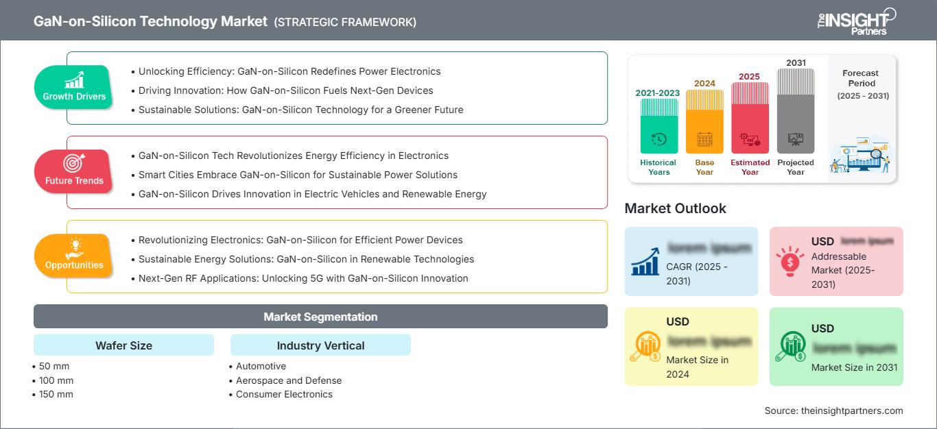
GaN-on-Silicon Technology Market: Strategic Insights
Regional Insights
North America Gan-on-Silicon Technology Market
North America holds a considerable Gan-on-Silicon Technology Market Share, with an estimated share of 28-32% in 2025. The regional market is forecast to have a CAGR of 13-15% from 2026 to 2034. The US forms the key demand driver in the region, which is driven by extensive procurements of defense electronics and innovations in consumer electronics. The region boasts a well-established infrastructure for semiconductor industry, excellent research organizations and government policies for developing compound semiconductors, which is evident in the CHIPS and Science Act in the region. Aerospace and defense emerge as one of the strongest segments in terms of demand, where Gan-on-silicon technologies are used in radar technology, electronic warfare equipment, and satellite communication.
U.S. Gan-on-Silicon Technology Market
The U.S. Market represents around 75–80% of the North American regional market in 2025 and is estimated to register a CAGR of 13–15% till 2034. The U.S. market is positively impacted by the presence of major players operating in the semiconductor, defense, and consumer electronics industries. Trends seen in applications suggest significant developments in automotive power electronics, aerospace and defense applications, and data centers infrastructure. The emphasis placed by the U.S. government on the development of the semiconductor industry within the region has created a positive environment for the development of GaN technology. Several fabrication units are being developed by several firms to expand their production capacities.
Europe Gan-on-Silicon Technology Market
The market share of Europe estimated to be between 22% and 26% in 2025, with a CAGR of 13-15% during the period from 2026 to 2034. The leading country in Europe is Germany, due to the presence of an advanced automobile industry and industrial automation industry, which has started adopting GaN-on-silicon technology for various applications related to power electronics and motor control. The next in line is the United Kingdom due to activities in aerospace and defense electronics, along with telecommunications infrastructure industry. France has its share due to aerospace and defense industries, whereas the countries of Italy and Spain are developing regions for the industry due to industrial applications and renewable energy sector.
APAC Gan-on-Silicon Technology Market
The Asia Pacific is the major market player in the global Gan on Silicon Technology Market, with a market share ranging from 38 to 42% by 2025 and a CAGR of 16 to 18% through 2034. The leading factor in the success of China as the leading market player in the region is the fact that China is the world’s biggest producer of consumer electronics as well as an electric vehicle maker. Japan contributes to the success of the region because of its capability in producing semiconductor materials and equipment. On the other hand, in South Korea, demand is created in this area due to consumer electronics and telecommunications infrastructure. India is considered as an emerging market due to the government initiatives that push for the manufacture of electronics products and usage of renewable energy sources.
Middle East & Africa Gan-on-Silicon Technology Market
The MEA region has become a rising market opportunity for Gan-on-Silicon Technology with Saudi Arabia and the UAE as leaders with the help of infrastructure and energy diversification efforts. The South African region offers opportunities in the industrial and telecommunication fields whereas ROFMEA (Rest of MEA) region is showing good growth in telecom and defense segments. It is forecasted that the region will experience growth at a CAGR of 12-14% in the period of 2026-2034 due to investment made in the development of smart cities, renewable energy, and telecom networks.
Segmentation Analysis
Wafer Size
The Wafer Size segment encompasses 50 mm, 100 mm, 150 mm, and 200 mm substrates, with the overall segment projected to grow at a CAGR of 14–16% from 2026 to 2034. Wafer size selection significantly influences manufacturing economics, device performance, and application suitability. The industry is progressively transitioning toward larger wafer formats to achieve cost efficiencies and higher production volumes, though smaller formats retain relevance for specialized applications and R&D purposes.
- 50 mm: The 50 mm wafer size serves niche applications in research and development, prototyping, and specialized low-volume production. This format remains relevant for emerging GaN technologies and academic research institutions exploring novel device architectures and materials combinations.
- 100 mm: The 100 mm wafer size supports mid-volume production for specialized power electronics and RF devices. This format is commonly utilized by foundries serving diverse industry verticals, offering a balance between manufacturing cost and production flexibility.
- 150 mm: The 150 mm wafer size held a substantial market share in 2025, representing an established production format with mature manufacturing processes. This size benefits from extensive installed equipment bases and proven process technologies across multiple applications.
- 200 mm: The 200 mm wafer size represents the fastest-growing format within the Market, driven by superior cost economics and compatibility with existing silicon fabrication infrastructure. This format enables higher device yields and lower per-unit costs.
Industry Vertical
The Industry Vertical segment includes Automotive, Aerospace and Defense, Consumer Electronics, and IT and Telecom, with the overall segment projected to grow at a CAGR of 14–16% from 2026 to 2034. Each vertical presents distinct requirements and adoption drivers, collectively contributing to the market's diversified growth profile.
- Automotive: The Automotive vertical is experiencing rapid adoption of Gan-on-Silicon Technology, driven by electric vehicle proliferation and demand for efficient power electronics. Applications include onboard chargers, DC-DC converters, and traction inverters, where GaN enables higher power density and reduced system costs.
- Aerospace and Defense: The Aerospace and Defense vertical represents a significant market for Gan-on-Silicon Technology, with applications in radar systems, electronic warfare, satellite communications, and avionics. The technology's high-frequency capabilities and reliability under extreme conditions drive adoption.
- Consumer Electronics: The Consumer Electronics vertical constitutes the largest market for Gan-on-Silicon Technology, driven by demand for compact, high-efficiency power adapters and fast-charging solutions. Smartphones, laptops, and wearable devices increasingly incorporate GaN-based power management components.
- IT and Telecom: The IT and Telecom vertical benefits from Gan-on-Silicon Technology's superior performance in high-frequency RF amplification and power conversion. Applications include 5G infrastructure, data center power supplies, and telecommunications equipment requiring high efficiency and reliability.
Opportunity Snapshot
| Industry Vertical | Revenue Contribution | Trend Tag | Adoption Stage |
|---|---|---|---|
| Automotive | High | EV Power | Scaling |
| Aerospace and Defense | Medium | RF Systems | Mature |
| Consumer Electronics | High | Fast Charging | Scaling |
| IT and Telecom | Medium | 5G Infrastructure | Scaling |
GaN-on-Silicon Technology Market Growth Drivers and Impact Analysis
Electric Vehicle Proliferation Driving GaN Power Electronics Adoption
The accelerating global transition to electric vehicles represents a primary growth driver for the Gan-on-Silicon Technology Market. EV manufacturers are increasingly adopting GaN-on-silicon solutions for onboard chargers, DC-DC converters, and traction inverters to achieve higher power density, reduce charging times, and improve overall vehicle efficiency. The technology enables smaller, lighter, and more efficient power systems compared to traditional silicon-based alternatives, addressing critical EV performance requirements. With global electric car sales reaching approximately 14 million units in 2023 and charging infrastructure expanding rapidly, the demand for GaN-based power electronics continues to intensify. The need for faster charging and extended vehicle range is expected to positively influence market growth throughout the forecast period.
5G Telecommunications Infrastructure Expansion
The global rollout of 5G telecommunications networks is creating substantial demand for high-frequency, high-power RF amplifiers, where Gan-on-Silicon Technology offers superior performance compared to traditional technologies. GaN-based RF components enable higher power output, improved efficiency, and better thermal management, making them essential for 5G base stations and infrastructure equipment. The technology's ability to operate at higher frequencies with reduced power loss supports the deployment of advanced wireless networks requiring increased data throughput and coverage. Telecommunications operators worldwide are investing heavily in 5G infrastructure, with GaN-on-silicon solutions playing a critical role in enabling network performance and efficiency goals.
Consumer Electronics Demand for Compact High-Efficiency Charging
The consumer electronics industry's pursuit of smaller form factors and faster charging capabilities has positioned Gan-on-Silicon Technology as a key enabler for next-generation power adapters and charging solutions. GaN-based power converters offer higher switching frequencies, enabling smaller magnetic components and reduced overall system size while maintaining or improving efficiency. Smartphone manufacturers, laptop producers, and accessory makers are increasingly incorporating GaN technology into their products to meet consumer expectations for rapid charging and portable designs. The global consumer electronics market, with smartphones generating the highest revenue at USD 467 billion in 2022, continues to drive adoption of GaN-based power management solutions.
GaN-on-Silicon Technology Market Future Trends
Transition to 200 mm and Larger Wafer Formats for Cost Reduction
The Gan-on-Silicon Technology Market Trends are experiencing a significant transition toward larger wafer formats, particularly 200 mm substrates, as manufacturers seek to achieve cost efficiencies and scale production. Multiple device makers qualified 200 mm GaN-on-silicon wafers during 2025, cutting die costs and enabling higher unit volumes. This transition leverages existing silicon fabrication infrastructure, reducing capital expenditure requirements and accelerating time-to-market for new products. The move to larger wafers is expected to drive further cost reductions, expand addressable applications, and support the technology's penetration into price-sensitive consumer and industrial segments.
Integration of GaN-on-Silicon in Data Center Power Infrastructure
The growing power demands of data centers and artificial intelligence computing infrastructure are creating new opportunities for Gan-on-Silicon Technology in power supply applications. GaN-based solutions offer higher efficiency and power density compared to traditional silicon-based power supplies, enabling data center operators to reduce energy consumption and cooling requirements. The technology's ability to operate at higher switching frequencies allows for more compact power supply designs, freeing up valuable rack space for computing equipment. As AI workloads continue to drive data center power consumption upward, GaN-on-silicon solutions are increasingly positioned as critical enablers for sustainable and efficient data center operations.
GaN-on-Silicon Technology Market Opportunities
Expansion into Emerging Renewable Energy Applications
The renewable energy sector presents substantial growth opportunities for Gan-on-Silicon Technology, particularly in solar inverters and wind turbine power electronics. GaN-based solutions enable higher energy conversion efficiency, reducing power losses and maximizing energy harvest from renewable sources. The technology's superior thermal performance and reliability under demanding operating conditions make it well-suited for renewable energy applications requiring long service life and minimal maintenance. With solar energy expected to account for 22% of global electricity generation by 2030, the addressable market for GaN-on-silicon solutions in renewable energy is poised for significant expansion.
Emerging MicroLED Display Manufacturing Applications
The development of GaN-on-silicon MicroLED microdisplays for augmented reality and near-eye display applications represents an emerging growth opportunity for the technology. GaN-on-silicon is compatible with CMOS processes, supports 200 mm and larger wafer manufacturing, and offers lower costs compared to traditional sapphire substrates. Collaborative projects, such as Germany's microPRO initiative involving SUSS MicroTec and other partners, are working to establish scalable production frameworks for next-generation microLED microdisplays. This application segment has the potential to open new revenue streams and diversify the Gan-on-Silicon Technology Market Forecast beyond traditional power electronics and RF applications.
Recent Developments
- August 2026: Power Integrations demonstrated the world’s first 2200 V GaN technology designed for next-generation high-voltage power systems. The technology targets advanced power conversion applications by enabling higher voltage operation, improved efficiency, and compact system designs for emerging industrial and energy infrastructure requirements.
- May 2025: Infineon Technologies AG expanded its GaN power portfolio with EasyPACK™ CoolGaN™ 650 V transistor modules for high-voltage applications. The solution is designed for data centers, renewable energy systems, and DC electric vehicle charging infrastructure, addressing demand for higher power efficiency and simplified system integration.
- December 2025: onsemi announced a collaboration with GlobalFoundries to develop next-generation 650 V lateral GaN power devices using a 200 mm GaN-on-silicon process. The initiative focuses on AI data centers, automotive, industrial, renewable energy, and aerospace applications by combining GaN technology with advanced power management solutions..
Frequently Asked Questions

- Comprehensive Market Sizing and Forecast Analysis
- Detailed Segmentation Analysis
- In-Depth Market Dynamics Assessment
- Regional and Country-Level Insights
- Competitive Landscape and Company Benchmarking
- Strategic Business Intelligence
Recent Reports
Testimonials

The Insight Partners provided valuable market intelligence that supported our global go-to-market strategy. Their team was professional, responsive, and attentive to our feedback, providing thoughtful analysis and helpful methodological clarifications throughout the project.
Junmo Kim Chief Financial Officer (CFO), Enertech Co., Ltd.
The Insight Partners' SCADA System Market report is comprehensive, with valuable insights on current trends and future forecasts. The team was highly professional, responsive, and supportive throughout. We are very satisfied and highly recommend their services.
RAN KEDEM Partner, Reali Technologies LTDs
I requested a report on a very specific software market and the team produced the report in a few days. The information was very relevant and well presented. I then requested some changes and additions to the report. The team was again very responsive and I got the final report in less than a week.
JEAN-HERVE JENN Chairman, Future Analytica
We worked with The Insight Partners for an important market study and forecast. They gave us clear insights into opportunities and risks, which helped shape our plans. Their research was easy to use and based on solid data. It helped us make smart, confident decisions. We highly recommend them.
PIYUSH NAGPAL Sr. Vice President, High Beam Global
The Insight Partners delivered insightful, well-structured market research with strong domain expertise. Their team was professional and responsive throughout. The user-friendly website made accessing industry reports seamless. We highly recommend them for reliable, high-quality research services
YUKIHIKO ADACHI CEO, Deep Blue, LLC.
This is the first time I have purchased a market report from The Insight Partners.While I was unsure at first, I visited their web site and felt more comfortable to take the risk and purchase a market report.I am completely satisfied with the quality of the report and customer service. I had several questions and comments with the initial report, but after a couple of dialogs over email with their analyst I believe I have a report that I can use as input to our strategic planning process.Thank you so much for taking the extra time and making this a positive experience.I will definitely recommend your service to others and you will be my first call when we need further market data.
JOHN SUZUKI President and Chief Executive Officer, Board Director, BK Technologies
I wish to appreciate your support and the professionalism you displayed in the course of attending to my request for information regarding to infectious disease IVD market in Nigeria. I appreciate your patience, your guidance, and the fact that you were willing to offer a discount, which eventually made it possible for us to close a deal. I look forward to engaging The Insight Partners in the future, all thanks to the impression you have created in me as a result of this first encounter.
DR CHIJIOKE ONYIA MANAGING DIRECTOR, PineCrest Healthcare Ltd.Reason to Buy
- Informed Decision-Making
- Understanding Market Dynamics
- Competitive Analysis
- Identifying Emerging Markets
- Customer Insights
- Market Forecasts
- Risk Mitigation
- Boosting Operational Efficiency
- Strategic Planning
- Investment Justification
- Tracking Industry Innovations
- Aligning with Regulatory Trends





 Get Free Sample for