
Semiconductor Defect Inspection System Market Size, Share & Forecast by 2034
Coverage: By Product Type (Wafer Inspection System, Mask Inspection System); Application (Consumer Electronics, Bank ATMs, Communications Infrastructure, Trains, Internet, Others) , and Geography (North America, Europe, Asia Pacific, and South and Central America)
- Status : Data Released
- Report Code : TIPRE00017006
- Category : Electronics and Semiconductor
- No. of Pages : 150
- Available Report Formats :


- Last update date : July 10, 2026


2025 Market Size
US$ 11,354.59 Mn
Base year value
2034 Forecast
US$ 17,864.44 Mn
Projected by 2034
CAGR 2026-2034
5.16 %
Growth rate
Addressable Market
US$ 132,533.32 Mn
(2026-2034)
The Semiconductor Defect Inspection System market size was estimated at $11.35 billion in 2025 and is forecasted to reach $17.86 billion in 2034, growing at a CAGR of 5.16%. The driving factors behind market growth include stringent tolerances for defects in advanced logic, memory, photomask, and wafer-level packaging processes, where defect inspection accuracy affects yields, cycle times, and manufacturing costs.
According to the Semiconductor Defect Inspection System Market report, North America is likely to grow at a 4.8–5.4% CAGR from 2026 to 2034, driven by reshoring programs, investment in AI fabs, and a focus on process control in leading-edge logic. The North American equipment industry is well-positioned for market growth due to proximity to key defect inspection technology providers, new U.S. fabs, and rising yield management requirements for advanced packaging and HPC supply chains.
Semiconductor Defect Inspection System Market Assessment and Insights
- North America: The region accounted for 24–27% share in 2025 and is projected to grow at a CAGR range of 4.8–5.4% during 2026–2034, supported by AI fabs and advanced packaging.
- US: The country represented 78–82% of North America in 2025 and is expected to grow at a CAGR range of 4.9–5.5% during 2026–2034.
- Europe: Europe held 16–19% share in 2025 and is forecast to expand at a CAGR range of 4.3–4.9%, led by Germany, the Netherlands, France, Italy, and the UK.
- Asia Pacific: APAC accounted for 49–53% share in 2025 and is expected to grow at a CAGR range of 5.4–6.0%, led by Taiwan, South Korea, China, and Japan.
- Largest Segment: Wafer Inspection System held 67–71% market share in 2025 and is expected to grow at a CAGR range of 5.0–5.6% during 2026–2034.
- High Growth Segment: Mask Inspection System held 29–33% market share in 2025 and is projected to expand at a CAGR range of 5.5–6.2% during 2026–2034.
- Key companies analyzed in detail: Applied Materials, Inc.; ASML Holding N.V.; Bruker Corporation; Camtek Ltd.; Hitachi High-Tech Corporation; KLA Corporation; Lasertec Corporation; Microtronic Inc.; Newport Corporation; NXP Semiconductors N.V.; Onto Innovation Inc.; TASMIT, Inc.; and Thermo Fisher Scientific Inc.
Source: The Insight Partners' analysis based on proprietary research, government publications, company annual reports, investor presentations, industry databases, and expert interviews.
According to the Semiconductor Defect Inspection System Market forecast, semiconductor defect inspection has moved beyond visual yield monitoring to become a process control function for devices below 7nm logic, high-bandwidth memory, advanced packaging, and EUV mask manufacturing. With smaller device geometries and more complex 3D designs, faster optical inspection, higher resolution e-beam review, and software-based classification will become key requirements. The Semiconductor Defect Inspection System Market share will depend more on installed base depth, analytics, services, and qualification in top-tier foundry and IDM sites.
Future investments will shift towards capacity expansions in APAC, fab incentives in the United States, European sovereignty plans, and Japan's materials and equipment cluster. SEMI announced record-breaking semiconductor equipment shipments in 2025 of US$135.1 billion, underscoring the importance of demand for inspections as manufacturers focus on yield improvement. Growth in the Semiconductor Defect Inspection System Market will depend on AI processors, HBM stacks, chiplets, and the regulation of resilient electronics supply chains.
Semiconductor Defect Inspection System Market Report Scope
| Report Attribute | Details |
|---|---|
| Market size in 2025 | US$ 11,354.59 Million |
| Market Size by 2034 | US$ 17,864.44 Million |
| Global CAGR (2026 - 2034) | 5.16% |
| Historical Data | 2021-2024 |
| Forecast period | 2026-2034 |
Semiconductor Defect Inspection System Market Analysis
Demand is rooted in the economics of yield loss. The more advanced the wafer, the more complicated the process, the longer the cycle time, and the more valuable the dies become. Therefore, early detection of defects becomes absolutely necessary. Wafer inspection remains key, as defects may occur in lithography, deposition, etch, and CMP, causing many to fail before electrical testing.
The value chain encompasses optics, sensors, vacuum systems, electron-beam columns, image-processing software, service engineers, and fab integration. The supply chain dynamics are affected by qualification cycle times and customer recipes. According to the Semiconductor Defect Inspection System Market report, tool replacement is not as cyclic as capital expenditure due to changes in processes requiring new inspection capabilities.
The competitive environment centers on companies with process-control intellectual property (IP) and fab reliability. The major players are KLA Corporation, Applied Materials, Inc., ASML Holding N.V., Lasertec Corporation, Hitachi High-Tech Corporation, and Onto Innovation Inc. They compete on sensitivity, speed, defect classification, and system availability, not price.
Investment in AI-related logic, HBM, hybrid bonding, and reticle inspection is among the Semiconductor Defect Inspection System Market trends. In 2025, Applied Materials released the PROVision 10 eBeam metrology system, and SEMI emphasized growth in front-end equipment. The strategic positioning relies on co-development with customers, software analytics, service density by regions, and the capability to serve different technology nodes of fabs.
● REPORT CUSTOMIZATION
Tailor This Report To Align With Your Specific Business Requirements
This report can be customized to align precisely with your business objectives, scope, and target markets. Customization options include tailored segmentation, geography, competitive analysis, and strategic insights to support informed decision-making.
Customize This Report →WHAT YOU CAN ADJUST
- ● Segmentations
- ● Geography
- ● Competitive Analysis
- ● Language Preferences
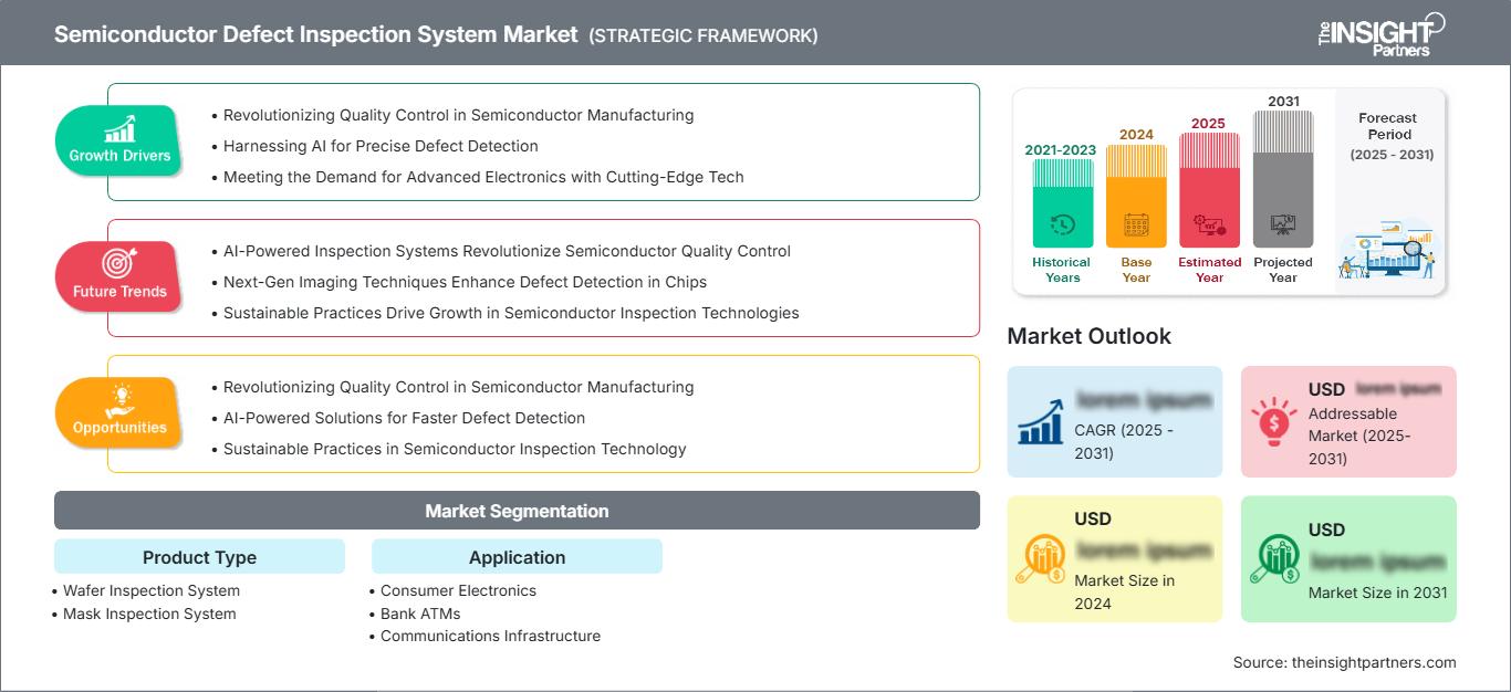
Semiconductor Defect Inspection System Market: Strategic Insights
Regional Insights
North America Semiconductor Defect Inspection System
North America accounted for 24–27% share in 2025 and is expected to register a CAGR range of 4.8–5.4% during 2026–2034. Growth is supported by CHIPS Act-linked fabs, AI accelerator manufacturing, advanced packaging pilots, and stronger domestic demand for process-control tools across logic, memory, and specialty semiconductor production.
Inspection adoption is strongest where defectivity affects high-value wafers and mission-critical electronics. The region hosts important supplier engineering, service, and customer collaboration centers, allowing faster recipe optimization. Semiconductor Defect Inspection System trends in North America also reflect higher investment in heterogeneous integration, where buried defects, voids, and alignment errors demand tighter monitoring.
U.S. Semiconductor Defect Inspection System Market
The U.S. represented 78–82% of North America in 2025 and is projected to grow at a CAGR range of 4.9–5.5% during 2026–2034. Domestic fab expansion, AI infrastructure demand, and defense-grade electronics requirements create stable pull for wafer and mask inspection platforms.
Company presence is significant, with Applied Materials, Inc., KLA Corporation, Onto Innovation Inc., Newport Corporation, and Thermo Fisher Scientific Inc. supporting equipment, optics, analytics, and service requirements. Application demand spans consumer electronics, communications infrastructure, bank ATMs, trains, and internet hardware, where semiconductor reliability supports uptime and cybersecurity-sensitive operations.
Europe Semiconductor Defect Inspection System Market
Europe held 16–19% share in 2025 and is expected to grow at a CAGR range of 4.3–4.9% during 2026–2034. The UK contributes through compound semiconductor research, design activity, and photonics-linked process development, supporting demand for inspection tools in specialty electronics and communications infrastructure.
Europe's dominant nation in terms of automotive electronics, industrial automation, power devices, and effective equipment integration capabilities is Germany. The acceptance of inspection depends on reliability in sectors such as trains, factory automation, and electrified mobility, where any problems can lead to safety, warranty, and production continuity issues.
France, Italy, Spain, and the Netherlands increase regional demand through aerospace electronics, analog devices, sensors, and lithography-related ecosystems. ASML Holding N.V. underscores Europe's strategic importance in patterning, while inspection vendors are favored due to EU policies on semiconductor autonomy and a reliable technology supply chain.
APAC Semiconductor Defect Inspection System Market
APAC accounted for 49–53% share in 2025 and is projected to grow at a CAGR range of 5.4–6.0% during 2026–2034. Taiwan and South Korea lead through advanced foundry, logic, DRAM, and HBM capacity.
China is still developing mature-node and selectively advanced-node capacity, which increases the need for wafer and mask inspection and local service support. Japan plays an important role in materials, optics, equipment engineering, and precision manufacturing.
India and Australia help via government-supported electronics ecosystem, research connections, and package development goals. The Scope of Semiconductor Defect Inspection System market in APAC region is increasing through government incentives, development of the Internet infrastructure, and higher quality standards for consumer and communication electronics.
Middle East & Africa Semiconductor Defect Inspection System Market
Middle East & Africa is projected to grow at a CAGR range of 4.0–4.6% during 2026–2034. Saudi Arabia and the UAE are exploring semiconductor-adjacent investments linked to data centers, energy diversification, and digital infrastructure.
South Africa contributes to regional demand via electronics assembly, telecommunications development, and industrial development. The demand from other MEA nations is still driven by projects in which inspection is linked to the reliability of imported chips and infrastructure rather than to wafer fabrication.
The UAE is the leading nation in terms of technology investment intensity in the region. Energy systems, internet access, and smart infrastructure increase dependence on semiconductor reliability, thereby indirectly creating demand for inspections.
Segmentation Analysis
Product Type
Product Type is expected to grow at a CAGR range of 5.1–5.7% during 2026–2034. Demand is shaped by the need to inspect both wafers and masks as lithography complexity increases. Wafer tools dominate installed spending, while mask inspection gains importance as EUV reticles, pellicles, and pattern fidelity become more critical to high-volume manufacturing.
- Wafer Inspection System holds the leading position because wafers require repeated inspection across front-end steps, enabling fabs to detect excursions early and reduce yield loss.
- Mask Inspection System is strategically important for EUV and advanced lithography, where reticle defects can replicate across many wafers and amplify downstream production losses.
Application
Application is expected to grow at a CAGR range of 5.0–5.6% during 2026–2034. Adoption is strongest where chip reliability, throughput, and component traceability influence customer outcomes. Consumer electronics provide volume scale, while communications infrastructure, bank ATMs, trains, and internet systems emphasize reliability, security, and long service life.
- Consumer Electronics contributes high-volume demand because smartphones, wearables, laptops, and home devices require compact chips manufactured with tight defect control and rapid yield learning.
- Bank ATMs require secure, reliable semiconductor components for transaction processing, display control, connectivity, and authentication hardware, making defect prevention important for uptime.
- Communications Infrastructure depends on high-performance logic, RF, optical, and power devices, where inspection supports reliability across 5G networks, data centers, and edge systems.
- Trains use semiconductors in signaling, traction control, safety systems, and passenger information platforms, making inspection-linked reliability essential for harsh operating environments.
- Internet applications rely on processors, memory, networking chips, and storage controllers, where defect control supports scalable cloud infrastructure and continuous digital service availability.
Opportunity Snapshot
| Application | Revenue Contribution | Trend Tag | Adoption Stage |
| Consumer Electronics | High | Compact Chips | Mature |
| Bank ATMs | Low | Secure Hardware | Mature |
| Communications Infrastructure | High | 5G Backhaul | Scaling |
| Trains | Medium | Rail Signaling | Scaling |
| Internet | High | Cloud Compute | Scaling |
Semiconductor Defect Inspection System Market Growth Drivers and Impact Analysis
Rising Process-Control Intensity in Advanced Nodes
Highly advanced logic, HBM, and 3D NAND technology fabrication add up to the process steps, thus increasing the frequency of defect inspections and complexity. According to SEMI, the worldwide billings of semiconductor equipment was US$ 135.1 billion in 2025, whereas the wafer processing equipment grew by 12%. This means that there is considerable investment in front-end control systems. Impact on the market is immediate – the fabs need highly sensitive, high speed, and high classification to decrease scrap rates and increase the ramp speed.
Growth of AI, HBM, and Advanced Packaging
AI-based accelerators, HBM stackup, and chiplet packages pose inspection challenges beyond traditional wafer surface inspections. Hybrid bonding, micro-bumps, RDLs, and buried interfaces introduce new defect mechanisms, including voids, delamination, warpage, and alignment issues. Such issues necessitate inspection solutions capable of optical and e-beam inspection along with analytics. The market implication of this is significant for companies providing solutions for front-end and packaging processes, since there will be demands for defect taxonomy consistency from fabrication to packaging and reliability qualification.
Regional Semiconductor Capacity Expansion
Government-backed manufacturing programs in the U.S., Europe, Japan, South Korea, Taiwan, China, and India are broadening the fab footprint and increasing demand for qualified inspection capacity. New fabs cannot reach profitable utilization without stable defect detection and yield-learning loops. This driver affects procurement timing because inspection tools are selected early in process qualification. It also expands service revenue opportunities, as suppliers must support recipe tuning, training, calibration, and uptime across geographically distributed production sites.
Semiconductor Defect Inspection System Market Future Trends
AI-Assisted Defect Classification
Future inspection platforms will rely more heavily on machine learning to classify nuisance defects, prioritize defects of interest, and shorten engineer review cycles. As fabs generate larger image datasets, software will become a differentiator alongside optics and sensors. This trend can reduce false positives, improve excursion response, and support faster process transfers between fabs. Vendors able to combine installed-base data, secure model training, and fab-specific recipe adaptation will strengthen switching barriers and improve recurring software-linked revenue.
Hybrid Metrology and Inspection Workflows
Manufacturers are expected to integrate optical inspection, e-beam review, metrology, and process data into hybrid workflows rather than treating each tool as an isolated station. This approach improves defect source tracing across deposition, etch, lithography, and packaging. The future value proposition will be broader than tool throughput; it will include actionable process intelligence. Suppliers with interoperable platforms, analytics software, and strong customer engineering teams will be better positioned to support complex multi-node fabs.
Semiconductor Defect Inspection System Market Opportunities
Advanced Packaging Inspection Toolsets
Advanced packaging creates a practical investment opportunity because defect modes differ from front-end wafer fabrication but are increasingly critical to AI and high-performance computing. Tool suppliers can target hybrid bonding, fan-out, interposers, and 2.5D/3D integration with inspection systems optimized for buried defects, bond quality, and alignment precision. Customers will value platforms that connect packaging data to upstream wafer history. Partnerships with OSATs, foundries, and substrate suppliers can accelerate qualification and create service-led revenue streams.
Localized Service and Recipe Engineering
As fabs expand across multiple regions, suppliers have an opportunity to differentiate through local service density, application labs, spare-part availability, and recipe engineering. Inspection tools require calibration, defect library updates, and close collaboration during ramp, making service proximity commercially important. Vendors that invest in regional demonstration centers and training programs can shorten customer adoption cycles. This opportunity is especially relevant in India, the U.S., Europe, and Southeast Asia, where new semiconductor ecosystems need process-control expertise.
Recent Developments
- May 2026: Tata Electronics, a pioneering leader in India’s electronics and semiconductor manufacturing sector, and ASML, one of the world’s leading semiconductor equipment manufacturing companies, announced the signing of a Memorandum of Understanding (MoU) to advance the semiconductor manufacturing ecosystem in India. Through this partnership, ASML will enable the establishment and successful ramp of Tata Electronics’ upcoming 300 mm (12 inch) semiconductor fab in Dholera, Gujarat. This collaboration is an important step in the context of the intensifying strategic collaboration between India and The Netherlands in the field of critical technologies, such as semiconductor technology.
- October 2025: Applied Materials, Inc. introduced next-generation chipmaking products for AI chips, including the PROVision 10 eBeam metrology system designed to improve yield in complex 3D chips through sub-nanometer resolution, fast throughput, and deep imaging capability.
- September 2025: KLA Corporation, in its 2025 stockholder letter, KLA reported record fiscal-year revenue of US$12.2 billion and noted that its Semi Process Control segment, including wafer inspection, reticle inspection, and metrology, increased 25% year over year, driven by AI, HBM, and advanced packaging demand.
Frequently Asked Questions

- Comprehensive Market Sizing and Forecast Analysis
- Detailed Segmentation Analysis
- In-Depth Market Dynamics Assessment
- Regional and Country-Level Insights
- Competitive Landscape and Company Benchmarking
- Strategic Business Intelligence
Recent Reports
Testimonials

The Insight Partners' SCADA System Market report is comprehensive, with valuable insights on current trends and future forecasts. The team was highly professional, responsive, and supportive throughout. We are very satisfied and highly recommend their services.
RAN KEDEM Partner, Reali Technologies LTDs
I requested a report on a very specific software market and the team produced the report in a few days. The information was very relevant and well presented. I then requested some changes and additions to the report. The team was again very responsive and I got the final report in less than a week.
JEAN-HERVE JENN Chairman, Future Analytica
We worked with The Insight Partners for an important market study and forecast. They gave us clear insights into opportunities and risks, which helped shape our plans. Their research was easy to use and based on solid data. It helped us make smart, confident decisions. We highly recommend them.
PIYUSH NAGPAL Sr. Vice President, High Beam Global
The Insight Partners delivered insightful, well-structured market research with strong domain expertise. Their team was professional and responsive throughout. The user-friendly website made accessing industry reports seamless. We highly recommend them for reliable, high-quality research services
YUKIHIKO ADACHI CEO, Deep Blue, LLC.
This is the first time I have purchased a market report from The Insight Partners.While I was unsure at first, I visited their web site and felt more comfortable to take the risk and purchase a market report.I am completely satisfied with the quality of the report and customer service. I had several questions and comments with the initial report, but after a couple of dialogs over email with their analyst I believe I have a report that I can use as input to our strategic planning process.Thank you so much for taking the extra time and making this a positive experience.I will definitely recommend your service to others and you will be my first call when we need further market data.
JOHN SUZUKI President and Chief Executive Officer, Board Director, BK Technologies
I wish to appreciate your support and the professionalism you displayed in the course of attending to my request for information regarding to infectious disease IVD market in Nigeria. I appreciate your patience, your guidance, and the fact that you were willing to offer a discount, which eventually made it possible for us to close a deal. I look forward to engaging The Insight Partners in the future, all thanks to the impression you have created in me as a result of this first encounter.
DR CHIJIOKE ONYIA MANAGING DIRECTOR, PineCrest Healthcare Ltd.Reason to Buy
- Informed Decision-Making
- Understanding Market Dynamics
- Competitive Analysis
- Identifying Emerging Markets
- Customer Insights
- Market Forecasts
- Risk Mitigation
- Boosting Operational Efficiency
- Strategic Planning
- Investment Justification
- Tracking Industry Innovations
- Aligning with Regulatory Trends





 Get Free Sample for