
Semiconductor Packaging Equipment Market Trends, Demand & Growth by 2034
Coverage: by Packaging Platform (Flip Chip, FIWLP, FOWLP, Others); Dimension (2D, 2.5D, 3D); Equipment Type (Deflashing Equipment, Molding Equipment, Solder Plating Equipment, Trim and Forming Equipment, Others); End-Use (Semiconductor Fabrication Plant/Foundry, Electronics Manufacturing, Testing Home) , and Geography (North America, Europe, Asia Pacific, and South and Central America)
- Status : Data Released
- Report Code : TIPRE00009013
- Category : Electronics and Semiconductor
- No. of Pages : 150
- Available Report Formats :


- Last update date : July 10, 2026


2025 Market Size
US$ 7.46 Bn
Base year value
2034 Forecast
US$ 12.7 Bn
Projected by 2034
CAGR 2026-2034
6.09 %
Growth rate
Addressable Market
US$ 91.29 Bn
(2026-2034)
The Semiconductor Packaging Equipment market size is expected to grow to US$ 12.7 Billion by 2034, rising from US$ 7.46 Billion in 2025, with a CAGR of 6.09% over the forecast period of 2026 to 2034. This growth is driven by the needs of advanced logic, high-bandwidth memory, chiplets, and package platform advancements to improve interconnect density, yield management, and thermal management within semiconductor ecosystem operations.
According to the Semiconductor Packaging Equipment market report, the North American market is expected to grow at a 5.4–5.9% CAGR between 2026–2034, driven by domestic semiconductor capacity buildout, AI accelerators, and outsourced assembly collaborations. The increase in foundry spending and advanced packaging pilot lines in the United States is driving growth in molding, plating, trim and form, and fan-out equipment.
Semiconductor Packaging Equipment Market Assessment and Insights
- North America: The region held a 17–20% Semiconductor Packaging Equipment market share in 2025 and is growing at a CAGR of 5.4–5.9% during 2026–2034, supported by reshoring, AI packaging capacity, and defense electronics reliability needs.
- US: The U.S. accounted for 78–82% of North America in 2025 and is growing at a CAGR of 5.5–6.0% during 2026–2034 as foundries add advanced assembly capabilities.
- Europe: Europe held an 8–11% share in 2025 and is growing at a CAGR of 4.6–5.2% during 2026–2034, led by Germany, France, the UK, Italy, and Spain.
- Asia Pacific: APAC held a 64–68% share in 2025 and is growing at a CAGR of 6.5–7.1% during 2026–2034, led by China, Taiwan, Japan, South Korea, and India.
- Largest Segment: Flip Chip held a 38–42% market share in 2025 and is growing at a CAGR of 5.8–6.4% during 2026–2034 due to high-volume processor and memory packages.
- High Growth Segment: 3D held a 14–17% market share in 2025 and is growing at a CAGR of 8.2–8.9% during 2026–2034 with HBM, hybrid bonding, and chiplet stacking.
- Key companies analyzed in detail: Advantest Corporation, Applied Materials, Inc., ASML Holding N.V., Hitachi High-Tech Corporation, KLA Corporation, Lam Research Corporation, Onto Innovation Inc., SCREEN Holdings Co., Ltd., Teradyne, Inc., Tokyo Electron Limited.
Source: The Insight Partners' analysis based on proprietary research, government publications, company annual reports, investor presentations, industry databases, and expert interviews.
While packaging was previously seen as an expensive back-end operation, today it is becoming a critical part of manufacturing. The Semiconductor Packaging Equipment Market is undergoing change as it transitions from traditional wire-bond packaging solutions to flip-chip, fan-out wafer-level packaging, and 2.5D/3D integration. According to SEMI, assembly and packaging equipment grew by 21% in 2025 because of increasing process intensity as AI chips, HBM, and advanced logic needed smaller overlay and increased inspection coverage.
The upcoming demand will be driven by fab localization, regional incentives, and the necessity to mitigate bottlenecks in the chain of AI and automotive semiconductor production. Emerging investment regions in the U.S., Japan, India, and Southeast Asia are establishing pilot and large-scale packaging production capacity. In light of government support of semiconductor independence and necessity of energy-efficient computers, the scope of the Semiconductor Packaging Equipment market extends beyond high-end foundries and includes electronics manufacturing and testing, and packaging subcontractors.
Semiconductor Packaging Equipment Market Report Scope
| Report Attribute | Details |
|---|---|
| Market size in 2025 | US$ 7.46 Billion |
| Market Size by 2034 | US$ 12.7 Billion |
| Global CAGR (2026 - 2034) | 6.09% |
| Historical Data | 2021-2024 |
| Forecast period | 2026-2034 |
Semiconductor Packaging Equipment Market Analysis
The semiconductor packaging equipment market forecast indicates that demand is influenced by AI accelerators, supercomputing, automotive electronics, and miniaturized end products. All these applications increase the need for shorter electrical connections, reduced power dissipation, and improved thermal management, making packaging platforms an important strategic consideration. According to the Semiconductor Packaging Equipment report, there is increasing demand for fan-out and flip-chip equipment, with the package density/cost trade-off being crucial in purchase decisions.
The ecosystem consists of foundries, outsourced semiconductor assembly and test companies, IDMs, materials suppliers, substrate suppliers, metrology companies, and test equipment manufacturers. The supply chain dynamics are sensitive to precision components, clean-room availability, and tool qualification timelines. Longer package development plans drive Semiconductor Packaging Equipment market growth; however, buyers are cautiously managing capital expenses because packaging equipment needs to match die, substrate, and test availability.
The competitive dynamics are dominated by diversified wafer fab and back-end equipment providers with process know-how, service networks for their installed base, and co-development programs with customers. Applied Materials, Inc., Tokyo Electron Limited, Lam Research Corporation, KLA Corporation, and ASML Holding N.V. are leveraging their front-end process experience to enter adjacent processes within packaging, whereas Advantest Corporation and Teradyne, Inc. are benefiting from increased testing due to assembly.
The Semiconductor Packaging Equipment market trends indicate that investors favor equipment suppliers with heterogeneous integration capabilities, panel-level process development capability, and yield analysis capabilities. Hitachi High-Tech Corporation, SCREEN Holdings Co., Ltd., and Onto Innovation Inc. are aligned with inspection, cleaning, and process control needs. Differentiation is becoming increasingly about equipment performance, field service support, and alignment with customer roadmaps beyond volume of equipment sold.
● REPORT CUSTOMIZATION
Tailor This Report To Align With Your Specific Business Requirements
This report can be customized to align precisely with your business objectives, scope, and target markets. Customization options include tailored segmentation, geography, competitive analysis, and strategic insights to support informed decision-making.
Customize This Report →WHAT YOU CAN ADJUST
- ● Segmentations
- ● Geography
- ● Competitive Analysis
- ● Language Preferences
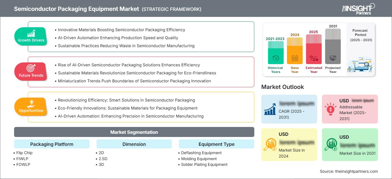
Semiconductor Packaging Equipment Market: Strategic Insights
Regional Insights
North America Semiconductor Packaging Equipment
In 2025, North America constituted a 17-20% Semiconductor Packaging Equipment market share and is projected to grow at a 5.4-5.9% CAGR through 2026-2034. The major demand drivers are foundries in the U.S., pilot lines for advanced packaging, defense electronics, and cloud AI infrastructure. Policies within the domestic market environment are facilitating investment in equipment that requires skilled molding, solder plating, deflashing, and inspection-capable packaging.
The purchase of regional packaging equipment is becoming increasingly reliant on reliability, traceability, and supplier proximity. There are several advantages for packaging equipment makers from the development of the U.S. and Canada semiconductor eco-system, yet the qualification cycles are long since the advanced packaging needs to satisfy stringent yield and thermal requirements. Therefore, the Semiconductor Packaging Equipment market share in North America is estimated to be stable.
U.S. Semiconductor Packaging Equipment Market
The Semiconductor Packaging Equipment market in the U.S. accounted for 78–82% of North America in 2025 and is growing at a 5.5–6.0% CAGR during 2026–2034. Foundry investments, chiplet development, and defense-grade microelectronics programs are raising demand for packaging platforms that support tighter interconnect pitch, higher power density, and improved process traceability across mission-critical devices.
Company presence is high because there are application labs, service teams, and customer engineering capabilities for major equipment suppliers located near the leading semiconductor hubs. Some of the companies that provide customer engineering for the US clients include Applied Materials, Inc., KLA Corporation, Lam Research Corporation, Teradyne, Inc., and Onto Innovation Inc. The technology has gained popularity in AI chips, aerospace electronics, and advanced automotive modules.
Europe Semiconductor Packaging Equipment Market
Europe has accounted for 8-11% of global demand in 2025 and forecasted to exhibit a 4.6-5.2% CAGR growth during 2026-2034. Germany drives regional demand as automotive power electronics, industrial automation, and sensors need robust packaging solutions that are resilient to thermal cycling and predictable performance over their lifespan.
The UK focuses on compound semiconductors, design-led packaging, and specialty electronics. It has less demand compared to Germany yet technologically advanced, especially photonics, defense electronics, and low-volume high-mix packages that need flexible molding, inspection, and trimming & forming equipment.
France, Italy, and Spain participate in aerospace applications, automotive electronics, and industrial manufacturing. Regional policies are supporting packaging-based R&D activities, however, slow electronics volumes restrict rapid expansion of equipment. Packaging suppliers that offer localized services and process knowledge are preferred by customers who emphasize reliability over cost-effective solutions.
APAC Semiconductor Packaging Equipment Market
The Semiconductor Packaging Equipment market in APAC held a 64–68% share in 2025 and is expected to grow at a 6.5–7.1% CAGR during 2026–2034. China, Taiwan, Japan, South Korea, India, and Australia support the region’s scale, with Taiwan leading advanced packaging intensity through AI and high-performance computing supply chains.
China’s mature node capabilities, South Korea’s HBM infrastructure, and Japan’s materials and equipment capabilities bolster the demand for molding, solder plating, deflashing, and inspection-related tools. India is developing through assembly benefits and increasing electronics manufacturing.
The driving policies comprise localizing the supply chain, export security, and national semiconductor strategies. Demand from industry continues to be diversified, including smartphones, servers, automotive electronics, and industrial automation, which make APAC the main revenue driver for the Semiconductor Packaging Equipment Market.
Middle East & Africa Semiconductor Packaging Equipment Market
The Semiconductor Packaging Equipment market in Middle East & Africa is forecast to grow at a 3.8–4.4% CAGR during 2026–2034, with Saudi Arabia leading regional interest through industrial diversification, digital infrastructure, and electronics assembly ambitions. Current demand remains project-based rather than broad-based.
The UAE is building technology infrastructure around data centers, logistics, and advanced manufacturing zones, which may create selective packaging and test opportunities. South Africa contributes through electronics repair, industrial systems, and mining automation components.
Rest of MEA demand is linked to energy, telecommunications, and infrastructure modernization. Equipment adoption will depend on partnerships with global OSATs and government-backed industrial programs rather than standalone semiconductor manufacturing scale.
Segmentation Analysis
Packaging Platform
The packaging platform segment in the Semiconductor Packaging Equipment market is expected to grow at a 6.1–6.7% CAGR during 2026–2034 as customers migrate toward higher interconnect density and better signal integrity. Platform selection depends on package complexity, die size, substrate availability, and yield economics. Flip chip remains the volume anchor, while fan-out solutions gain relevance where form factor and redistribution layer flexibility are critical.
- Flip Chip holds the strongest installed base because it supports processors, memory, and communication chips needing high I/O density, mature assembly flows, and predictable thermal performance in volume manufacturing.
- FIWLP is used where compact package footprint, thin profile, and cost-efficient wafer-level processing matter, especially in mobile, connectivity, and sensor devices requiring space-saving integration.
- FOWLP is gaining strategic importance in advanced consumer electronics and AI-adjacent devices because redistribution flexibility improves electrical performance without relying on conventional substrate scaling.
Dimension
The dimension segment is projected to grow at a 6.4–7.0% CAGR during 2026–2034. Device makers are balancing cost, performance, and manufacturability across 2D, 2.5D, and 3D architectures. 2D packages remain essential for mature applications, while 2.5D and 3D formats are becoming more important for bandwidth-intensive AI, graphics, networking, and memory applications.
- 2D packaging remains widely used in mainstream electronics because it offers lower process complexity, established equipment availability, and stable yields for cost-sensitive semiconductor device categories.
- 2.5D packaging supports interposer-based integration where processors and memory must communicate at high speed, making it important for AI accelerators and data-center silicon.
- 3D packaging is strategically important for vertical stacking, HBM integration, and chiplet roadmaps because it shortens interconnects and improves performance per unit area.
Equipment Type
The equipment type segment is expected to grow at a 5.9–6.5% CAGR during 2026–2034. Demand is distributed across process steps that protect package integrity, improve electrical connectivity, and prepare components for board-level assembly. Tool selection is influenced by package materials, throughput, defect sensitivity, and compatibility with advanced wafer-level and panel-level workflows.
- Deflashing Equipment is essential for removing excess mold compound and improving package reliability, particularly in high-volume assembly lines where cosmetic defects can signal deeper process instability.
- Molding Equipment supports package protection and thermal management, making it central to power devices, automotive modules, and advanced packages exposed to higher operating stress.
- Solder Plating Equipment enables reliable interconnect formation and remains important as bump uniformity, corrosion control, and fine-pitch compatibility become more demanding in advanced packages.
- Trim and Forming Equipment prepares packaged devices for final assembly, supporting lead integrity, dimensional consistency, and downstream automation in electronics manufacturing lines.
End-Use
The end-use segment is projected to grow at a 6.0–6.6% CAGR during 2026–2034. Semiconductor fabrication plants and foundries drive high-specification tool demand, while electronics manufacturing and testing homes broaden the customer base. Purchasing criteria vary by throughput, package mix, qualification burden, and ability to support rapid product transitions without yield loss.
- Semiconductor Fabrication Plant/Foundry customers prioritize process precision, supplier co-development, and scalable capacity because packaging increasingly determines final device performance and manufacturability.
- Electronics Manufacturing customers require flexible equipment that can handle varied package formats, cost targets, and rapid production changes across consumer, industrial, and automotive assemblies.
- Testing Home demand is linked to rising test coverage after packaging, especially for AI, HBM, and automotive devices where failures are costly and reliability expectations are strict.
Opportunity Snapshot
| End-Use | Revenue Contribution | Trend Tag | Adoption Stage |
| Semiconductor Fabrication Plant/Foundry | High | Chiplet Lines | Scaling |
| Electronics Manufacturing | Medium | Package Mix | Mature |
| Testing Home | Medium | HBM Test | Scaling |
Semiconductor Packaging Equipment Market Growth Drivers and Impact Analysis
AI and HBM Packages Increase Back-End Process Intensity
Denser interconnects, thinner wafers, precise molding, and test coverage are among the requirements for advanced AI chips and high-bandwidth memory. According to SEMI, there was a 55% increase in test equipment billings and a 21% increase in assembly and packaging equipment sales in 2025, illustrating the rising importance of advanced devices in the back end. The effects manifest as prolonged qualification cycles, higher tool utilization rates, and greater emphasis on process control. Suppliers of equipment who can minimize warpage, residue, and interconnect defects can secure high-value orders.
Foundry Localization Expands Packaging Capacity Requirements
National programs aimed at fostering semiconductor development are spurring foundries and IDMs to establish full manufacturing capabilities locally, including assembly and testing. This involves changing sourcing strategies from large-scale sites in Asia to distributed capacity in North America, Europe, Japan, and India. It is not just about the increase in the number of tools being sourced, but also about the need for local application expertise and support. Having application centers and experience in their installed base gives suppliers an advantage as the dependence on far-off packaging bottlenecks decreases.
Advanced Consumer and Automotive Electronics Raise Reliability Needs
Automotive electronics, smartphones, wearables, and industrial controls require packages that survive heat, vibration, miniaturization, and continuous operation. These requirements raise demand for molding equipment, solder plating systems, trim and forming tools, and inspection workflows that can prevent latent defects. The impact is strongest where manufacturers face warranty exposure and strict quality audits. As electronics content per vehicle and device density increase, packaging equipment becomes a reliability investment rather than only a production cost.
Semiconductor Packaging Equipment Market Future Trends
Panel-Level Fan-Out Moves Toward Production Readiness
Panel-level fan-out is expected to gain attention as customers seek better area utilization and lower unit costs for large advanced packages. The transition from wafer formats to panels is technically difficult because warpage, alignment, and yield control become harder at larger dimensions. However, collaborative development among equipment, materials, and substrate suppliers is moving the approach closer to practical adoption. If process stability improves, panel-level packaging could reshape tool specifications for lithography, molding, cleaning, and inspection over the next decade.
Hybrid Bonding Becomes Central to 3D Integration
Hybrid bonding is moving from specialized deployments toward broader relevance in 3D device integration because it enables finer pitch and shorter interconnects than solder-based approaches. Future equipment demand will emphasize ultra-clean surfaces, accurate alignment, wafer thinning, and metrology capable of detecting defects before stacking. The trend supports the Semiconductor Packaging Equipment trends around chiplet architectures and energy-efficient computing. Suppliers that integrate bonding, cleaning, inspection, and process analytics will be better placed for next-generation package roadmaps.
Semiconductor Packaging Equipment Market Opportunities
Service-Led Expansion for Regional Packaging Lines
As packaging capacity spreads across new geographies, customers will need faster tool installation, recipe transfer, operator training, and maintenance support. This creates an opportunity for equipment suppliers to combine hardware sales with service contracts, process optimization, and uptime guarantees. Regional service depth can influence vendor selection because packaging defects are expensive to diagnose after downstream assembly. Companies that invest in local application centers and remote monitoring can improve customer retention while building recurring revenue beyond initial tool shipments.
Integrated Metrology for Yield-Sensitive Advanced Packages
Advanced packages contain more interfaces, materials, and process steps, increasing the risk of hidden defects. Equipment vendors can capture opportunity by embedding metrology, inspection, and data analytics into packaging workflows rather than treating quality checks as separate steps. This approach supports faster root-cause analysis and improves yield learning for fan-out, flip chip, and 3D packages. Customers pursuing the Semiconductor Packaging Equipment Market for high-value AI and automotive devices are likely to pay for systems that reduce scrap and qualification delays.
Recent Developments
- June 2026: Applied Materials, Inc., the pioneer of materials engineering in the semiconductor industry, announced the launch of its new range of semiconductor manufacturing equipment. These equipment designed for creating advanced 3D chip structures used in AI applications.
- March 2025: Toray Engineering Co., Ltd launched the UC5000. It is a highly precise semiconductor packaging machine (bonder) used in panel level packaging(PLP).
- September 2025: Resonac Corporation made an announcement about the establishment of "JOINT3," a co-creation evaluation system made up of a consortium consisting of Resonac and 27 other companies in Japan, the USA, Singapore, and other countries. These companies, which are all major global players in the semiconductor industry, will work together to develop optimized materials, equipment, and design tools suitable for making panel-level organic interposer semiconductors using a prototype production line for making 515 x 510mm panel-level organic interposers.
Frequently Asked Questions

- Comprehensive Market Sizing and Forecast Analysis
- Detailed Segmentation Analysis
- In-Depth Market Dynamics Assessment
- Regional and Country-Level Insights
- Competitive Landscape and Company Benchmarking
- Strategic Business Intelligence
Recent Reports
Testimonials

The Insight Partners provided valuable market intelligence that supported our global go-to-market strategy. Their team was professional, responsive, and attentive to our feedback, providing thoughtful analysis and helpful methodological clarifications throughout the project.
Junmo Kim Chief Financial Officer (CFO), Enertech Co., Ltd.
The Insight Partners' SCADA System Market report is comprehensive, with valuable insights on current trends and future forecasts. The team was highly professional, responsive, and supportive throughout. We are very satisfied and highly recommend their services.
RAN KEDEM Partner, Reali Technologies LTDs
I requested a report on a very specific software market and the team produced the report in a few days. The information was very relevant and well presented. I then requested some changes and additions to the report. The team was again very responsive and I got the final report in less than a week.
JEAN-HERVE JENN Chairman, Future Analytica
We worked with The Insight Partners for an important market study and forecast. They gave us clear insights into opportunities and risks, which helped shape our plans. Their research was easy to use and based on solid data. It helped us make smart, confident decisions. We highly recommend them.
PIYUSH NAGPAL Sr. Vice President, High Beam Global
The Insight Partners delivered insightful, well-structured market research with strong domain expertise. Their team was professional and responsive throughout. The user-friendly website made accessing industry reports seamless. We highly recommend them for reliable, high-quality research services
YUKIHIKO ADACHI CEO, Deep Blue, LLC.
This is the first time I have purchased a market report from The Insight Partners.While I was unsure at first, I visited their web site and felt more comfortable to take the risk and purchase a market report.I am completely satisfied with the quality of the report and customer service. I had several questions and comments with the initial report, but after a couple of dialogs over email with their analyst I believe I have a report that I can use as input to our strategic planning process.Thank you so much for taking the extra time and making this a positive experience.I will definitely recommend your service to others and you will be my first call when we need further market data.
JOHN SUZUKI President and Chief Executive Officer, Board Director, BK Technologies
I wish to appreciate your support and the professionalism you displayed in the course of attending to my request for information regarding to infectious disease IVD market in Nigeria. I appreciate your patience, your guidance, and the fact that you were willing to offer a discount, which eventually made it possible for us to close a deal. I look forward to engaging The Insight Partners in the future, all thanks to the impression you have created in me as a result of this first encounter.
DR CHIJIOKE ONYIA MANAGING DIRECTOR, PineCrest Healthcare Ltd.Reason to Buy
- Informed Decision-Making
- Understanding Market Dynamics
- Competitive Analysis
- Identifying Emerging Markets
- Customer Insights
- Market Forecasts
- Risk Mitigation
- Boosting Operational Efficiency
- Strategic Planning
- Investment Justification
- Tracking Industry Innovations
- Aligning with Regulatory Trends





 Get Free Sample for