
Semiconductor Photolithography Equipment Market Trends, Demand & Growth by 2034
Coverage: By Type (Advanced Packaging, MEMS (Microelectromechanical systems) Devices, LED (Light Emitting Diode) Devices); Application (Consumer Electronics, Industrial, Commercial, Others) , and Geography (North America, Europe, Asia Pacific, and South and Central America)
- Status : Data Released
- Report Code : TIPRE00017169
- Category : Electronics and Semiconductor
- No. of Pages : 150
- Available Report Formats :


- Last update date : July 10, 2026


2025 Market Size
US$ 24.19 Bn
Base year value
2034 Forecast
US$ 41.44 Bn
Projected by 2034
CAGR 2026-2034
6.17 %
Growth rate
Addressable Market
US$ 297.21 Bn
(2026-2034)
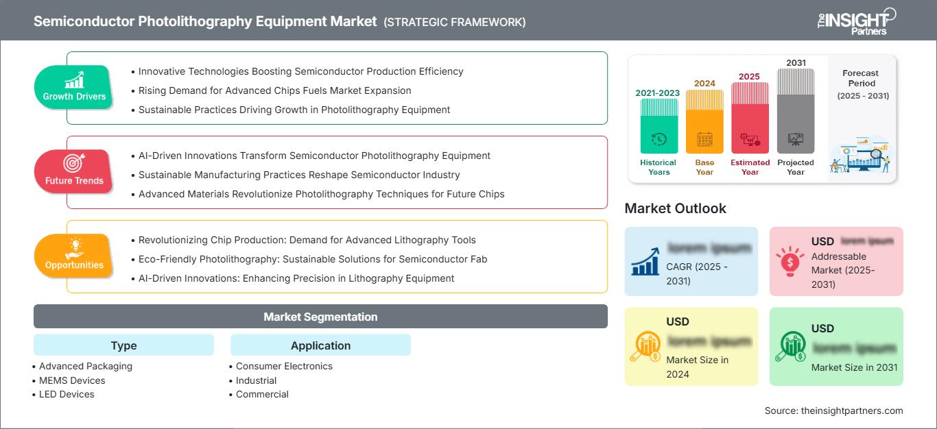
The semiconductor photolithography equipment market size will increase from US$ 24.19 Billion in 2025 to US$ 41.44 Billion by 2034, with a CAGR of 6.17% from 2026 to 2034. It includes exposure and patterning tools employed in wafer processing and certain back-end operations, where the market dynamics will be driven by device scaling, heterogeneous integration, and capacity expansion in memory, logic, MEMS, LED, and advanced packaging segments.
According to the semiconductor photolithography equipment market report, North America is set to grow at a 5.8%-6.4% CAGR through 2034, driven by fab incentives, advanced packaging spending, and the need for domestically secured semiconductor manufacturing capacity. The U.S. funding, foundry builds, and compound semiconductor efforts are boosting the pull-through of equipment solutions, whereas customers remain focused on productivity, overlay precision, and serviceability in mature and leading edge fabs.
Semiconductor Photolithography Equipment Market Assessment and Insights
- North America: The region accounted for 24–27% semiconductor photolithography equipment market share in 2025 and is projected to grow at a CAGR of 5.8–6.4% during 2026–2034, driven by U.S. fab incentives and packaging capacity.
- US: The country represented 78–82% of North America in 2025 and is forecast to grow at a CAGR of 5.9–6.5% during 2026–2034.
- Europe: Europe held 11–14% share in 2025 and is expected to grow at a CAGR of 4.8–5.4% during 2026–2034, led by Germany, France, the Netherlands, and Italy.
- Asia Pacific: APAC captured 55–59% share in 2025 and is projected to expand at a CAGR of 6.6–7.2% during 2026–2034, led by Taiwan, China, South Korea, and Japan.
- Largest Segment: Advanced Packaging held 44–48% market share in 2025 and is expected to grow at a CAGR of 6.5–7.1% during 2026–2034.
- High Growth Segment: MEMS Devices held 27–31% market share in 2025 and is projected to grow at a CAGR of 6.9–7.5% during 2026–2034.
- Key companies analyzed in detail: Applied Materials, Inc.; ASML Holding N.V.; Canon Inc.; JEOL Ltd.; Nikon Corporation; NuFlare Technology, Inc.; S-Cubed; SÜSS MICROTEC SE; Tokyo Electron Limited; Vistec Electron Beam GmbH.
Source: The Insight Partners' analysis based on proprietary research, government publications, company annual reports, investor presentations, industry databases, and expert interviews.
The technology shift will see lithography spend migrate from the scaling front-end patterning environment to a broader patterning environment. EUV and immersion DUV will continue to be critical for advanced logic and memory fabrication, while i-line, KrF, e-beam, and mask aligners serve the compound semiconductors, MEMS, LED, and packaging segments. Therefore, the growth in the Semiconductor Photolithography Equipment Market is driven by transistor density and the increasing number of lithography steps in chiplet architectures.
The forward investments will move towards regions which provide subsidies, process engineering talent, and customers. Capacity will increase in India, the U.S., Japan, and some European countries, but Asia will remain the manufacturing region. The scope of the Semiconductor Photolithography Equipment will widen due to the need of high throughput exposure equipment for advanced packaging, sensors manufacturing, and power device fabs.
Semiconductor Photolithography Equipment Market Report Scope
| Report Attribute | Details |
|---|---|
| Market size in 2025 | US$ 24.19 Billion |
| Market Size by 2034 | US$ 41.44 Billion |
| Global CAGR (2026 - 2034) | 6.17% |
| Historical Data | 2021-2024 |
| Forecast period | 2026-2034 |
Semiconductor Photolithography Equipment Market Analysis
Demand is driven by fabs’ need for greater-density patterning, higher yields, and overlay stability across larger volumes of wafer start-ups. According to SEMI, global semiconductor equipment bookings reached US$135.1 billion in 2025, representing a 15% increase over the previous year. Meanwhile, sales of wafer-processing equipment grew by 12%, implying significant investment in front-end process equipment. This situation contributes to the Semiconductor Photolithography Equipment Market research among state-of-the-art and specialty device manufacturing processes.
The market ecosystem comprises optics, light sources, stages, masks, resists, metrology, and services. Supply in the market is concentrated since photolithography equipment needs exacting modules, lengthy qualification periods, and custom integration solutions. The Semiconductor Photolithography Equipment Market trends indicate a shift towards platforms that emphasize throughput, uptime, computational corrections, and service options, particularly driven by emerging lithography levels in advanced packaging.
The market environment is structurally concentrated for advanced nodes and broad for specialty lithography processes. ASML Holding N.V. controls the EUV and high-end immersion lithography, while Canon Inc. and Nikon Corporation play an active role in i-line, KrF, Nanoimprint, and packaging exposure processes. NuFlare Technology, Inc., JEOL Ltd., and Vistec Electron Beam GmbH provide the needs for e-beam and mask-writing technologies.
The semiconductor photolithography equipment market forecast indicates that strategic positioning of the market players is moving towards service revenues, co-development, and application-specific exposure systems. Applied Materials, Inc. and Tokyo Electron Limited affect adjacent process modules, while SÜSS MICROTEC SE and S-Cubed target the advanced packaging, MEMS, and specialty device flows. Such an organizational structure creates structural dependence of Semiconductor Photolithography Equipment share on the installed base and service capabilities.
● REPORT CUSTOMIZATION
Tailor This Report To Align With Your Specific Business Requirements
This report can be customized to align precisely with your business objectives, scope, and target markets. Customization options include tailored segmentation, geography, competitive analysis, and strategic insights to support informed decision-making.
Customize This Report →WHAT YOU CAN ADJUST
- ● Segmentations
- ● Geography
- ● Competitive Analysis
- ● Language Preferences
Semiconductor Photolithography Equipment Market: Strategic Insights
Regional Insights
North America Semiconductor Photolithography Equipment
North America held a market share of 24–27% in 2025 and is expected to grow at a 5.8–6.4% CAGR through 2026–2034. North America gains from fab construction related to the CHIPS Act, packaging initiatives, and supplier localization. Equipment purchases occur in logic, memory, compound semiconductor, and defense-related manufacturing applications, where yield management and sourcing are critical.
The end-users in the region are investing in mature-node and advanced-node production, which helps create demand for equipment such as scanners, steppers, and mask writers, as well as maintenance services. The size of the Semiconductor Photolithography Equipment market in North America is driven by applications in AI accelerators, automotive electronics, and local packaging infrastructure.
U.S. Semiconductor Photolithography Equipment Market
The U.S. represented 78–82% of North America in 2025 and is expected to grow at a 5.9–6.5% CAGR during 2026–2034. New fabs in Arizona, Texas, Ohio, and New York are creating multi-year equipment demand. Applications include advanced logic, memory support, silicon photonics, MEMS, and heterogeneous integration for AI and high-performance computing.
The presence of the companies is strengthened by the services offered by ASML Holding N.V., Applied Materials, Inc., process integration, and customers in America who need fast field assistance. Adoption by the U.S. highlights productivity, security in logistics, and packaging lithography. In addition, the industry gets a boost from the university consortia and national labs that expedite process learning.
Europe Semiconductor Photolithography Equipment Market
Europe has a market share of 11–14% and is expected to register a 4.8–5.4% CAGR in the period 2026–2034. It is led by The Netherlands via ASML Holding N.V.'s lithography ecosystem and Germany for the automotive, industrial, and power semiconductor applications. Resilience programs are enhancing tool localization, photonics capability, and specialty node investment.
The UK is part of the ecosystem due to its compound semiconductor clusters and photonic development to meet lithography needs in RF, sensors, and optoelectronics. Germany is the leading country in equipment consumption due to automotive electronics, industrial automation, and power device applications needing i-line, KrF, and mask alignment equipment.
France, Italy, and Spain are driving demand for the equipment due to microelectronics clusters, silicon carbide, MEMS, and government fab programs. Growth in the European Semiconductor Photolithography Equipment Market will be driven more by strategic factors than by volume factors compared to APAC.
APAC Semiconductor Photolithography Equipment Market
APAC accounted for 55–59% share in 2025 and is forecast to grow at a 6.6–7.2% CAGR during 2026–2034. Taiwan leads advanced foundry investments, while South Korea drives memory and HBM-related lithography intensity.
China continues to be an important demand hub for mature node capacity, MEMS, LED, and tool substitution. Japan is also contributing to the market through its equipment providers, materials, and logic technology development programs.
India and Australia are developing in terms of their semiconductors programs, packaging, and research capabilities. APAC continues to be the primary volume region for the deployment of Semiconductor Photolithography Equipment, driven by industrial policies, demand for artificial intelligence, and electronics manufacturing.
Middle East & Africa Semiconductor Photolithography Equipment Market
Middle East & Africa is projected to grow at a 4.2–4.8% CAGR during 2026–2034, from a small base. Saudi Arabia and the UAE are evaluating semiconductor ecosystems linked to AI infrastructure, energy diversification, and industrial technology strategies.
South Africa contributes through electronics manufacturing, research, and mining-linked sensor applications, while Rest of MEA demand is mainly tied to infrastructure digitization. The UAE is the leading regional country because data-center and technology investment create stronger semiconductor adjacency.
Energy transition, grid monitoring, and industrial automation can create selective demand for MEMS and power-device lithography. However, most regional activity will remain ecosystem-building rather than high-volume wafer fabrication through the forecast period.
Segmentation Analysis
Type
Type is projected to grow at a 6.3–6.9% CAGR during 2026–2034 as lithography demand diversifies across advanced packaging, MEMS, and LED manufacturing. The segment is shaped by wafer-level packaging, sensor miniaturization, and optoelectronic device scaling, where exposure accuracy, substrate handling, and productivity matter more than node scaling alone.
- Advanced Packaging leads demand as chiplet integration, redistribution layers, and HBM packaging require accurate overlay, large-field exposure, and scalable throughput for high-value AI and data-center devices.
- MEMS Devices show strong strategic importance because automotive sensors, medical devices, microphones, and inertial systems need repeatable lithography on varied substrates and process flows.
- LED Devices remain important in compound semiconductor production, with lithography supporting mini-LED, micro-LED, automotive lighting, and display backplane requirements across sapphire and gallium nitride substrates.
Application
Application is expected to grow at a 5.9–6.5% CAGR during 2026–2034 as electronics demand becomes more lithography-intensive across consumer, industrial, and commercial use cases. The segment reflects the Semiconductor Photolithography Equipment growth opportunity created by connected devices, automation, energy systems, and compute infrastructure that need smaller, more efficient, and more reliable components.
- Consumer Electronics remains a major demand pool because smartphones, wearables, displays, and connected home devices require image sensors, MEMS microphones, power devices, and compact processors.
- Industrial applications are expanding as factory automation, robotics, grid equipment, and predictive-maintenance systems increase demand for sensors, power semiconductors, and ruggedized electronic components.
- Commercial applications include data centers, communication infrastructure, enterprise systems, and professional electronics, where photolithography supports advanced logic, memory interfaces, and high-reliability packaging.
Opportunity Snapshot
| Application | Revenue Contribution | Trend Tag | Adoption Stage |
| Consumer Electronics | High | Smart Devices | Mature |
| Industrial | Medium | Factory Sensors | Scaling |
| Commercial | High | AI Servers | Scaling |
Semiconductor Photolithography Equipment Market Growth Drivers and Impact Analysis
AI and HBM Capacity Increasing Lithography Intensity
AI accelerators, high-bandwidth memory, and chiplet architectures require more lithography steps across front-end and back-end process flows. SEMI’s 2025 equipment data showed test billings up 55% and assembly and packaging equipment up 21%, reflecting the broader capital cycle around AI devices. This driver increases demand for exposure systems used in redistribution layers, interposers, and memory-related process modules, strengthening the Semiconductor Photolithography Equipment Market beyond conventional wafer scaling.
Regional Fab Incentives Supporting Tool Installation
Government incentives in the U.S., Europe, Japan, India, and South Korea are reducing capital risk for new fabs and packaging facilities. These programs do not guarantee immediate equipment orders, but they improve project financing, local workforce development, and supplier commitments. As capacity moves from announcements to construction and qualification, lithography suppliers benefit from multi-year installation, service, and upgrade cycles tied to secure semiconductor production and regional supply-chain resilience.
Advanced Packaging Moving Lithography into Back-End Flows
Advanced packaging is making photolithography a critical back-end capability rather than only a front-end wafer process. Fan-out, 2.5D interposers, through-silicon vias, and chiplet interconnects require controlled exposure across larger fields and varied substrates. This changes purchasing criteria toward overlay, substrate handling, and cost per good package. The shift supports vendors with packaging-focused steppers, mask aligners, and process integration expertise, especially where AI and HPC devices need high-density interconnects.
Semiconductor Photolithography Equipment Market Future Trends
High-NA EUV Transition for Advanced Logic
High-NA EUV adoption will gradually reshape advanced-node lithography roadmaps by reducing multi-patterning complexity and improving pattern fidelity at smaller dimensions. Early deployment will remain limited to leading logic and memory customers because tool cost, resist readiness, mask infrastructure, and process learning are substantial barriers. Over time, the technology can increase equipment value per fab and reinforce service intensity, making lifecycle support, computational lithography, and optics reliability central to supplier differentiation.
Panel-Level and Large-Field Exposure Expansion
Panel-level packaging and large-field exposure are expected to gain attention as device makers seek lower cost per interconnect and higher throughput for chiplet-based systems. Unlike front-end scaling, this trend depends on substrate warpage control, alignment across larger areas, and compatibility with redistribution-layer materials. Tool suppliers that adapt optics, stages, and handling systems for panels can address a growing production niche linked to AI servers, communications hardware, and high-density consumer electronics.
Semiconductor Photolithography Equipment Market Opportunities
Service-Led Revenue from Installed Base Optimization
Large installed bases of DUV, i-line, and packaging lithography tools create a durable opportunity for upgrades, refurbishments, software correction, and uptime services. Many fabs prefer extending qualified tools for mature nodes, MEMS, power devices, and packaging because process changes are costly. Vendors can capture recurring revenue by improving overlay control, energy efficiency, and predictive maintenance, while customers gain capacity without full greenfield equipment replacement. This makes lifecycle management a strategic growth channel.
Specialty Devices for Electrification and Sensing
Electrification, industrial sensing, medical devices, and optical systems are expanding demand for specialty semiconductors that do not always require leading-edge EUV. Silicon carbide, gallium nitride, MEMS, image sensors, and micro-LED devices need lithography platforms optimized for substrate variation and process flexibility. Suppliers can pursue this opportunity through modular steppers, mask aligners, and e-beam systems tailored to smaller-batch, high-mix production where reliability and application support outweigh absolute resolution leadership.
Recent Developments
- May 2026: Tata Electronics with ASML have made an announcement about the signing of an MoU (Memorandum of Understanding). This collaboration will help Tata Electronics to successfully establish and ramp up their upcoming semiconductor fab facility in Dholera, Gujarat that uses the 300 mm (12-inch) wafers. This collaboration is important considering the fact that there is increased strategic cooperation between India and The Netherlands in the domain of critical technologies like semiconductors.
- June 2026: Nikon Corporation is working on a high-productivity digital lithography system for use in advanced packaging technologies in back-end process technologies of semiconductors manufacturing. The resolution offered is 1.5 µm*1 (L/S) *2 and it will further improve the productivity. The throughput improvement is estimated to be greater than 30 %, going from 50 panels per hour, which is the throughput of DSP-100 digital lithography system*3, to 65 panels per hour or more*4. The product launch is planned in fiscal year 2027.
- September 2024: Canon Inc. said it would be delivering its most sophisticated lithography system, the FPA-1200NZ2C nanoimprint lithography (NIL) system for semiconductor fabrication, to the Texas Institute for Electronics (TIE), a semiconductor industry consortium located in Texas.
Frequently Asked Questions

- Comprehensive Market Sizing and Forecast Analysis
- Detailed Segmentation Analysis
- In-Depth Market Dynamics Assessment
- Regional and Country-Level Insights
- Competitive Landscape and Company Benchmarking
- Strategic Business Intelligence
Recent Reports
Testimonials

The Insight Partners provided valuable market intelligence that supported our global go-to-market strategy. Their team was professional, responsive, and attentive to our feedback, providing thoughtful analysis and helpful methodological clarifications throughout the project.
Junmo Kim Chief Financial Officer (CFO), Enertech Co., Ltd.
The Insight Partners' SCADA System Market report is comprehensive, with valuable insights on current trends and future forecasts. The team was highly professional, responsive, and supportive throughout. We are very satisfied and highly recommend their services.
RAN KEDEM Partner, Reali Technologies LTDs
I requested a report on a very specific software market and the team produced the report in a few days. The information was very relevant and well presented. I then requested some changes and additions to the report. The team was again very responsive and I got the final report in less than a week.
JEAN-HERVE JENN Chairman, Future Analytica
We worked with The Insight Partners for an important market study and forecast. They gave us clear insights into opportunities and risks, which helped shape our plans. Their research was easy to use and based on solid data. It helped us make smart, confident decisions. We highly recommend them.
PIYUSH NAGPAL Sr. Vice President, High Beam Global
The Insight Partners delivered insightful, well-structured market research with strong domain expertise. Their team was professional and responsive throughout. The user-friendly website made accessing industry reports seamless. We highly recommend them for reliable, high-quality research services
YUKIHIKO ADACHI CEO, Deep Blue, LLC.
This is the first time I have purchased a market report from The Insight Partners.While I was unsure at first, I visited their web site and felt more comfortable to take the risk and purchase a market report.I am completely satisfied with the quality of the report and customer service. I had several questions and comments with the initial report, but after a couple of dialogs over email with their analyst I believe I have a report that I can use as input to our strategic planning process.Thank you so much for taking the extra time and making this a positive experience.I will definitely recommend your service to others and you will be my first call when we need further market data.
JOHN SUZUKI President and Chief Executive Officer, Board Director, BK Technologies
I wish to appreciate your support and the professionalism you displayed in the course of attending to my request for information regarding to infectious disease IVD market in Nigeria. I appreciate your patience, your guidance, and the fact that you were willing to offer a discount, which eventually made it possible for us to close a deal. I look forward to engaging The Insight Partners in the future, all thanks to the impression you have created in me as a result of this first encounter.
DR CHIJIOKE ONYIA MANAGING DIRECTOR, PineCrest Healthcare Ltd.Reason to Buy
- Informed Decision-Making
- Understanding Market Dynamics
- Competitive Analysis
- Identifying Emerging Markets
- Customer Insights
- Market Forecasts
- Risk Mitigation
- Boosting Operational Efficiency
- Strategic Planning
- Investment Justification
- Tracking Industry Innovations
- Aligning with Regulatory Trends





 Get Free Sample for