
Atomic Force Microscopy Market Demand, Size & Forecast by 2034
Coverage: By Offering (Atomic Force Microscopes, Probes, Software); Grade (Industrial Grade AFM, Research-Grade AFM); Application (Materials Science, Life Sciences, Semiconductor and Electronics, Academics, Others) , and Geography (North America, Europe, Asia Pacific, and South and Central America)
- Status : Data Released
- Report Code : TIPRE00007262
- Category : Electronics and Semiconductor
- No. of Pages : 150
- Available Report Formats :


- Last update date : July 17, 2026


2025 Market Size
US$ 556.84 Mn
Base year value
2034 Forecast
US$ 1,019.11 Mn
Projected by 2034
CAGR 2026-2034
6.95 %
Growth rate
Addressable Market
US$ 7,118.57 Mn
(2026-2034)
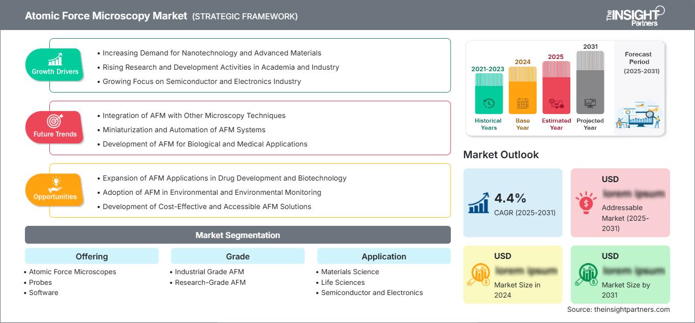
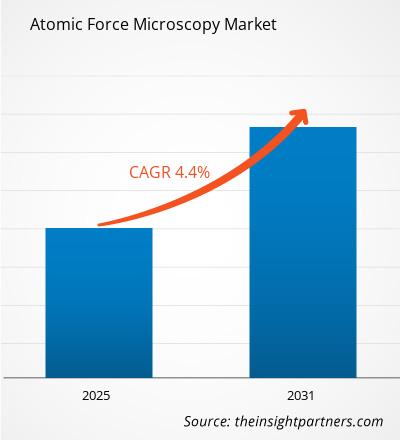
The Atomic Force Microscopy Market size is projected to grow from US$ 556.84 Million in 2025 to US$ 1,019.11 Million by 2034; it is expected to register a CAGR of 6.95% during 2026–2034. Adoption is fueled by nanotechnology applications in semiconductors, material sciences, life sciences, and academia, where atomic-scale surface characterization is beneficial in increasing reliability, repeatability, and defect analysis of products.
The North American region is estimated to experience a CAGR of 6.6-7.0% from 2026 to 2034 due to the presence of nanotechnology research funding, advanced capabilities for semiconductors manufacturing, and a high number of research facilities that utilize AFM. Demand will also be boosted by chip fabrication initiatives, instrumentation centers of universities, and life science institutes making use of the technology.
Atomic Force Microscopy Market Assessment and Insights
- North America: The region accounted for 34–36% of the Atomic Force Microscopy Market share in 2025 and is projected to grow at a 6.6–7.0% CAGR between 2026–2034, led by semiconductor metrology, nanomedicine, and university instrumentation programs.
- US: The country represented 78–82% of North America in 2025 and is expected to grow at a 6.7–7.1% CAGR between 2026–2034, supported by chip, biotech, and advanced materials ecosystems.
- Europe: Europe held 25–27% share in 2025 and is forecast to grow at a 6.1–6.5% CAGR between 2026–2034, with Germany, the UK, France, Italy, and Spain leading research and industrial adoption.
- Asia Pacific: APAC captured 28–30% share in 2025 and is projected to grow at a 7.3–7.7% CAGR between 2026–2034, driven by China, Japan, South Korea, India, and Australia.
- Largest Segment: Atomic force microscopes held 58–62% market share in 2025 and are expected to grow at a 6.4–6.8% CAGR between 2026–2034 as laboratories prioritize platform capability.
- High Growth Segment: Industrial Grade AFM held 42–46% market share in 2025 and is projected to grow at a 7.4–7.8% CAGR between 2026–2034, supported by fab automation.
- Key companies analyzed in detail: AFMWorkshop, Anton Paar GmbH, Bruker Corporation, Hitachi High-Tech Corporation, Nanonics Imaging Ltd., Nanosurf AG, NT-MDT Spectrum Instruments, Oxford Instruments plc, Park Systems Corp., and WITec GmbH.
Source: The Insight Partners' analysis based on proprietary research, government publications, company annual reports, investor presentations, industry databases, and expert interviews.
The Atomic Force Microscopy Market has evolved from research microscopy to nanometrology solutions, which are integrated with fast scanning, automated probe handling, environmental control, and image interpretation via software. The production dynamics will be characterized by increasing connections among instrumentation manufacturers, probe providers, semiconductor fabrication plants, and core facilities at universities. With decreasing size and growing complexity of devices and materials, AFM becomes an important tool for measuring parameters such as roughness, adhesion, modulus, electrical properties, and contamination on the nanometer scale.
Emerging demand during the forecast period will be driven by APAC semiconductor hubs, European initiatives on quantum materials, and biomedical engineering laboratories in North America. The market will benefit from regulatory tailwinds associated with clean manufacturing of electronic devices, evaluation of nanomaterials and reproducibility of biomedical studies. The Atomic Force Microscopy Market report shows that customers will prefer automation, probes for specific applications, and software to minimize the need for expertise.
Atomic Force Microscopy Market Report Scope
| Report Attribute | Details |
|---|---|
| Market size in 2025 | US$ 556.84 Million |
| Market Size by 2034 | US$ 1,019.11 Million |
| Global CAGR (2026 - 2034) | 6.95% |
| Historical Data | 2021-2024 |
| Forecast period | 2026-2034 |
Atomic Force Microscopy Market Analysis
The existence of demand for AFM comes from the inability of optical and electron microscopes to fully elucidate mechanical, electrical, and biological processes at nanoscale. The semiconductor industry uses AFM in line edge roughness, three-dimensional surface characterization, and defect review in addition to AFM's material laboratory application for polymers, batteries, coatings, ceramics, and thin films. Life science users appreciate AFM's capability of operating in a liquid environment during investigations of cell membrane, protein, DNA, and biomolecular interactions.
The value chain consists of piezo scanner makers, cantilevers and probes suppliers, vibration isolation equipment, software vendors, distributors and field services providers. The supply situation remains highly specialized due to precise parts, clean assembly and calibration knowledge limiting quick scale up. Thus, development of the Atomic Force Microscopy Market is determined by the instrument reliability, probe availability and application support.
The market has a relatively moderate level of concentration with Bruker Corporation and Park Systems Corp. having a lead in high end research and industry instruments whereas Oxford Instruments plc, Hitachi High-Tech Corporation, Nanosurf AG, and Anton Paar GmbH concentrating on niche academic and industry uses. AFMWorkshop, Nanonics Imaging Ltd., NT-MDT Spectrum Instruments, and WITec GmbH serve niche and customized needs like modular, near-field, and correlative arrangements.
Current investment trends include automation, large sample holders, nanoscale infrared spectroscopy, high-speed imaging, and analytics which help make AFM usable outside experienced users. Positioning strategies become more reliant on installation base servicing, probe supply, and software upgrades rather than hardware sales. The share of Atomic Force Microscopy Market will tend to move to vendors offering accurate measurements with high throughput in semiconductor and advanced materials industries.
● REPORT CUSTOMIZATION
Tailor This Report To Align With Your Specific Business Requirements
This report can be customized to align precisely with your business objectives, scope, and target markets. Customization options include tailored segmentation, geography, competitive analysis, and strategic insights to support informed decision-making.
Customize This Report →WHAT YOU CAN ADJUST
- ● Segmentations
- ● Geography
- ● Competitive Analysis
- ● Language Preferences
Atomic Force Microscopy Market: Strategic Insights
Regional Insights
North America Atomic Force Microscopy Market
North America held 34–36% share in 2025 and is expected to grow at a 6.6–7.0% CAGR through 2034. The demand basis is derived from semiconductor research and development, analysis of nanomaterials, and biomedical engineering. The procurement cycle in the United States is supported by federal science organizations and national laboratories along with cleanrooms at universities, whereas Canadian organizations participate in photonics, polymer science, and life sciences research.
The structural elements include chip placement, packaging technology, testing quality assurance of thin films, and surface analysis without conductive coating. The existing service infrastructure within the area guarantees low downtime of costly instruments. The customers use automatic AFMs because they enable the analysis of large samples and reproducible process flow.
U.S. Atomic Force Microscopy Market
The U.S. represented 78–82% of North America in 2025 and is forecast to grow at a 6.7–7.1% CAGR between 2026 and 2034. Demand factors include semiconductor process control, quantum materials initiatives, and biomedical nanomechanics applications. Bruker Corporation, Park Systems Corp., Oxford Instruments plc, and Hitachi High-Tech Corporation have very good commercial outreach due to direct sales, application labs, and service coverage.
The areas where development is happening include wafer inspection, 2D materials, energy storage interfaces, biomolecular force spectroscopy, and polymer surface science. Universities and instrumentation centers remain important customers owing to the fact that AFM is interdisciplinary in one single platform. The commercial users have an interest in the automation of the recipe, cleanroom procedure, and comparable metrology output between labs.
Europe Atomic Force Microscopy Market
Europe accounted for 25–27% share in 2025 and is projected to grow at a 6.1–6.5% CAGR through 2034. Demand for Nanoscience in academia, batteries and biomedical imaging in the United Kingdom comes from laboratories that require highly flexible AFM instruments for research purposes.
Germany leads Europe as a result of materials for automotive industry, precision engineering, semiconductor instrumentation, along with highly developed Max Planck and Fraunhofer institutes. Buyers in Germany favor industrial AFM instruments resistant to wear and tear for use in coatings, microelectronics, polymers and surface reliability testing.
France, Italy, and Spain participate through materials institutions, photonics clusters, pharmaceutical research, and university nanotechnology centers. The demand in Europe depends on collaborative funding for research, high quality requirements, and upgrading of laboratory equipment for studies of thin films, catalysis, membranes, and advanced surface technologies.
APAC Atomic Force Microscopy Market
APAC held 28–30% share in 2025 and is expected to grow at a 7.3–7.7% CAGR through 2034. China is the market leader due to semiconductor localization, university nanoscience, and battery materials.
Demand in Japan and South Korea is buoyed by electronics, displays, precision materials, and advanced packaging. The needs of these countries’ industrial customers include reliable automated instrumentation for surface topography and defect inspection.
Demand in India and Australia is fueled by publically-funded research infrastructure, clean-energy materials, biomedical engineering, and university procurement. Support for indigenous electronics, quantum technology, and university modernization helps assure longer term regional adoption.
Middle East & Africa Atomic Force Microscopy Market
Middle East & Africa is projected to grow at a 5.4–5.8% CAGR through 2034. Saudi Arabia is the leading country, supported by university research parks, petrochemical materials analysis, and investments in advanced manufacturing.
Demand for AFMs in the UAE is being created through nanotechnology research, clean energy materials, and infrastructure laboratories. The applications of AFMs are increasing in areas such as coatings, membranes, solar materials, and corrosion, all associated with diversification.
In South Africa and the RoMEA, AFM use is still mainly in academia and government research procurement. Growth is slow due to lack of trained personnel and budget limitations.
Segmentation Analysis
Offering
The offering segment is expected to grow at a 6.5–6.9% CAGR between 2026 and 2034. Hardware remains the revenue anchor, but probes and software increasingly shape recurring value. Buyers assess total measurement capability, including scan stability, probe lifetime, analytics, and training, making integrated offerings more competitive in the Atomic Force Microscopy Market trends landscape.
- Atomic force microscopes dominate revenue because platform purchases carry high average selling prices and determine laboratory capability, especially for semiconductor, materials science, and life science users.
- Probes generate recurring demand as users require application-specific cantilevers for mechanical mapping, electrical characterization, liquid imaging, and high-resolution surface measurements across varied sample environments.
- Software is strategically important because automated workflows, image correction, force-curve analysis, and data management reduce operator dependency and improve reproducibility across multi-user laboratories.
Grade
The grade segment is forecast to grow at a 6.8–7.2% CAGR between 2026 and 2034. Research-grade systems retain broad academic demand, while industrial-grade AFM gains momentum as semiconductor, electronics, and quality-control users require automation, large-sample compatibility, repeatability, and lower measurement variability. This shift improves the Atomic Force Microscopy Market forecast.
- Industrial Grade AFM is strategically important for fabs and production laboratories because it supports automated recipes, wafer-scale samples, higher throughput, and standardized metrology outputs.
- Research-Grade AFM remains essential in universities and institutes where flexibility, multimode operation, environmental control, and broad sample compatibility matter more than production-line throughput.
Application
The application segment is projected to grow at a 6.7–7.1% CAGR during 2026–2034. Materials science and semiconductor applications lead procurement because surface roughness, mechanical response, and nanoscale defect information directly influence product development. Life sciences and academics provide diversified demand, making application breadth a key stabilizer for the Atomic Force Microscopy Market.
- Materials Science uses AFM to evaluate polymers, coatings, composites, catalysts, membranes, and battery interfaces where nanoscale roughness, adhesion, and modulus affect product performance.
- Life Sciences demand focuses on cell surfaces, proteins, DNA, biomolecular interactions, and liquid-environment imaging, supporting research in mechanobiology, drug delivery, and diagnostics.
- Semiconductor and Electronics applications emphasize wafer inspection, thin-film metrology, failure analysis, 2D materials, and advanced packaging where sub-nanometer measurements support process control.
- Academics remain a stable user base because AFM platforms support teaching, multidisciplinary research, shared instrumentation facilities, and early-stage exploration of new materials and biological systems.
Opportunity Snapshot
| Application | Revenue Contribution | Trend Tag | Adoption Stage |
| Materials Science | High | Thin Films | Mature |
| Life Sciences | Medium | Cell Mechanics | Scaling |
| Semiconductor and Electronics | High | Wafer Metrology | Scaling |
| Academics | Medium | Shared Labs | Mature |
| Others | Low | Specialty QC | Emerging |
Atomic Force Microscopy Market Growth Drivers and Impact Analysis
Semiconductor Miniaturization Raises Metrology Requirements
Chip, 3D packaging, and compound semiconductor processes require surface data at resolutions achievable by standard optics. AFM provides data on line edge roughness, trench depth, film thickness, and contamination at nanoscale resolution. With decreasing process windows in fabs, there is a shift from laboratory testing to metrology. This means increased usage of automated stages, large samples, vibration control, and recipe generation based on nanoscale data.
Nanomaterials Research Expands Instrument Utilization
Studies involving batteries, catalysts, polymers, membranes, coating, and 2D materials require an understanding of surface morphology. AFM is able to characterize roughness, modulus, adhesion, conductivity, and defects that exist locally. The ability to do this helps in speeding up the process of formulation and failure analysis. With growing investments by both private and public labs in clean energy, advanced manufacturing, and functional materials, there is increased use of AFM in facilities.
Life Science Imaging Moves Toward Native Conditions
Biological labs require equipment to analyze soft samples in solution. AFM allows the investigation of cells, membranes, proteins, and other biological assemblies without the need for staining and preparation in vacuum conditions. The biggest market influence is achieved in the fields of mechanobiology, drug delivery, biomaterials, and diagnostics, in which forces are studied along with fluorescence and electron microscopy. Companies offering solutions to handle and analyze the data will have an opportunity to reach more biomedical users.
Atomic Force Microscopy Market Future Trends
AI-Assisted AFM Workflows Become Standard
The next-generation machines would include the incorporation of AI in scan optimization, artifact identification, feature identification, and reporting automation. This is going to minimize the reliance on skilled individuals and make AFM feasible for use in multi-user labs and industrial quality control groups. The software will also assist in comparing images from different instruments and locations. Manufacturers with an advanced analytics ecosystem can generate more revenue through subscriptions, upgrades, and application software libraries.
Correlative Nanometrology Gains Adoption
AFM will be increasingly used in conjunction with techniques such as Raman, infrared, optical, and electron microscopy so as to combine topography with chemical, mechanical, and electrical properties. Correlation techniques will particularly prove helpful when analyzing defects in semiconductors, blends of polymers, bio-materials, and batteries, among others, in which case single technique would not be sufficient to explain performance.
Atomic Force Microscopy Market Opportunities
Industrial AFM for Advanced Packaging Lines
There is an obvious investment opportunity in advanced packaging due to the need for accurate surface and defect data when it comes to hybrid bonding, redistribution layer, micro bumps, and heterogeneous integration. AFM companies may address packaging facilities by providing automated recipes, wafer compatibility, and data related to process control. Collaboration with equipment integrators and semiconductor research centers will speed up the qualification processes. The investment opportunities are not limited to just selling instruments but may include probes, maintenance, training, and analytics.
Application-Specific Probe and Software Bundles
There is more of a desire for validated workflows than individual instrumentation. Suppliers can create workflow packages that contain reagents, sample holders, calibration materials, and methods for battery testing, polymer testing, living cell testing, wafer testing, and coating testing. These workflow kits will save time in method development and will increase the confidence of non-expert users. From a business perspective, workflow kits will generate higher profit margins and consumable income, as well as make it easier to sell products through distributors.
Recent Developments
- February 2025: Park Systems, a global leader in atomic force microscopy (AFM), has unveiled an expanded FX Large Sample AFM series at SEMICON Korea 2025. Building on the success of Park FX200, which debuted at SEMICON West 2024 and has since gained strong market traction in Germany, Japan, and Korea, Park Systems introduces Park FX300 for 300 mm wafer analysis, alongside Park FX200 IR and FX300 IR, which integrate infrared (IR) spectroscopy, pushing the boundaries of large-sample AFM technology.
- December 2025: Surfmera has announced its advanced portfolio of atomic force microscopes (AFM), establishing the company as a leader in nanoscale imaging and measurement solutions. Designed to support researchers and industries, these advanced instruments enable new insights into material properties, chemical composition, and physical phenomena at the atomic and molecular levels. By integrating robust engineering with user-focused software and automation, Surfmera’s platforms simplify complex nanoscale analysis into efficient, reproducible, and insightful workflows.
- May 2025: Oxford Instruments introduces the Jupiter Discovery Atomic Force Microscope (AFM) to deliver best-in-class performance and exceptional ease of use. This versatile, large-sample AFM ensures that scientists in both academia and industry can attain the higher resolution, repeatability, and throughput they require while empowering even users with minimal training to achieve their research goals.
Frequently Asked Questions

- Comprehensive Market Sizing and Forecast Analysis
- Detailed Segmentation Analysis
- In-Depth Market Dynamics Assessment
- Regional and Country-Level Insights
- Competitive Landscape and Company Benchmarking
- Strategic Business Intelligence
Recent Reports
Testimonials

The Insight Partners' SCADA System Market report is comprehensive, with valuable insights on current trends and future forecasts. The team was highly professional, responsive, and supportive throughout. We are very satisfied and highly recommend their services.
RAN KEDEM Partner, Reali Technologies LTDs
I requested a report on a very specific software market and the team produced the report in a few days. The information was very relevant and well presented. I then requested some changes and additions to the report. The team was again very responsive and I got the final report in less than a week.
JEAN-HERVE JENN Chairman, Future Analytica
We worked with The Insight Partners for an important market study and forecast. They gave us clear insights into opportunities and risks, which helped shape our plans. Their research was easy to use and based on solid data. It helped us make smart, confident decisions. We highly recommend them.
PIYUSH NAGPAL Sr. Vice President, High Beam Global
The Insight Partners delivered insightful, well-structured market research with strong domain expertise. Their team was professional and responsive throughout. The user-friendly website made accessing industry reports seamless. We highly recommend them for reliable, high-quality research services
YUKIHIKO ADACHI CEO, Deep Blue, LLC.
This is the first time I have purchased a market report from The Insight Partners.While I was unsure at first, I visited their web site and felt more comfortable to take the risk and purchase a market report.I am completely satisfied with the quality of the report and customer service. I had several questions and comments with the initial report, but after a couple of dialogs over email with their analyst I believe I have a report that I can use as input to our strategic planning process.Thank you so much for taking the extra time and making this a positive experience.I will definitely recommend your service to others and you will be my first call when we need further market data.
JOHN SUZUKI President and Chief Executive Officer, Board Director, BK Technologies
I wish to appreciate your support and the professionalism you displayed in the course of attending to my request for information regarding to infectious disease IVD market in Nigeria. I appreciate your patience, your guidance, and the fact that you were willing to offer a discount, which eventually made it possible for us to close a deal. I look forward to engaging The Insight Partners in the future, all thanks to the impression you have created in me as a result of this first encounter.
DR CHIJIOKE ONYIA MANAGING DIRECTOR, PineCrest Healthcare Ltd.Reason to Buy
- Informed Decision-Making
- Understanding Market Dynamics
- Competitive Analysis
- Identifying Emerging Markets
- Customer Insights
- Market Forecasts
- Risk Mitigation
- Boosting Operational Efficiency
- Strategic Planning
- Investment Justification
- Tracking Industry Innovations
- Aligning with Regulatory Trends





 Get Free Sample for