
GaN Substrate and Wafer Market Size, Share & Forecast by 2034
Coverage: By Application (LEDs, Lasers, RF Device, Transistors, Others); End User (IT and Telecom, Healthcare, Automobiles, Consumer Electronics, Military and Defense, Others) , and Geography (North America, Europe, Asia Pacific, and South and Central America)
- Status : Data Released
- Report Code : TIPRE00026587
- Category : Electronics and Semiconductor
- No. of Pages : 150
- Available Report Formats :


- Last update date : August 18, 2026


2025 Market Size
US$ 175.63 Mn
Base year value
2034 Forecast
US$ 425.71 Mn
Projected by 2034
CAGR 2026-2034
10.34 %
Growth rate
Addressable Market
US$ 2,669.50 Mn
(2026-2034)
The GaN Substrate and Wafer market was valued at US$ 175.63 million in 2025 and is expected to reach US$ 425.71 million by 2034; it is estimated to record a CAGR of 10.34% during 2026-2034.
GaN Substrate and Wafer Market Assessment and Insights
- North America: Share in 2025 is modelled at 26–29%, with CAGR between 2026–2034 at 10.8–11.6%, supported by defense electronics, data-center power conversion, telecom infrastructure, and compound-semiconductor investment.
- US: The country holds 82–86% of North American demand in 2025 and grows at a 10.9–11.7% CAGR through 2034.
- Europe: Share in 2025 is modelled at 19–22%, with CAGR between 2026–2034 at 9.8–10.6%; Germany leads, while France, the UK, Italy, and Spain contribute automotive, aerospace, and industrial demand.
- Asia Pacific: Share in 2025 is modelled at 43–47%, with CAGR between 2026–2034 at 12.4–13.2%; Japan leads high-quality native substrates, while China and South Korea scale LEDs, RF, and electronics manufacturing.
- Largest Segment: LEDs represent a modelled 36–40% market share in 2025 and expand at a 9.8–10.6% CAGR through 2034.
- High Growth Segment: Transistors hold a modelled 21–25% market share in 2025 and expand at a 13.4–14.2% CAGR through 2034.
- Key companies analyzed in detail: AIXTRON SE, Soitec Belgium N.V., Fujitsu Limited, GaN Systems Inc., Kyocera Corporation, Mitsubishi Chemical Group Corporation, Compagnie de Saint-Gobain S.A., Soitec S.A., Sumitomo Electric Industries, Ltd., and Toshiba Corporation.
Source: The Insight Partners' analysis based on proprietary research, government publications, company annual reports, investor presentations, industry databases, and expert interviews.
The commercial interest in substrate development shifted from sapphire wafers used for making LEDs to the development of GaN-on-silicon, GaN-on-SiC, and native GaN substrates for high power electronics. More die can be obtained per wafer due to higher wafer size, improvements in hydride vapor phase epitaxy process, lower dislocation densities, and greater control of bowing. Commercialization is technology specific because of specific equipment needs for crystal growth, cutting, polishing, epi-ready, and defects testing. Device makers are increasingly testing substrates with epitaxy to avoid thermal mismatch, cracking, and yields loss.
Until 2034, there should be investments into six-inch native GaN, 200 mm GaN-on-silicon, thermal management systems, and regional pilot lines. Asia Pacific region is still the production center while North America and Europe will strengthen their sovereign semiconductor manufacturing capability. Higher energy efficiency regulations, telecommunication densification, vehicle electrification, and military enhancement provide additional opportunities for adoption. Companies which are capable to provide good crystal quality, gallium supply chain security, and application engineering will enjoy long cycle time for customer programs.
GaN Substrate and Wafer Market Report Scope
| Report Attribute | Details |
|---|---|
| Market size in 2025 | US$ 175.63 Million |
| Market Size by 2034 | US$ 425.71 Million |
| Global CAGR (2026 - 2034) | 10.34% |
| Historical Data | 2021-2024 |
| Forecast period | 2026-2034 |
GaN Substrate and Wafer Market Analysis
The GaN Substrate Wafer Market has been spurred by applications that need high breakdown voltage, fast switching, high-frequency operation, and effective heat dissipation capability. RF amplifiers, laser diodes, advanced LEDs, chargers, inverters, and power transistors are examples of devices that make use of these physical properties to create miniature parts with reduced losses. The supply chain consists of raw material suppliers, crystal growers, wafer producers, epitaxial growers, deposition equipment makers, foundries, end-device designers, and OEMs.
The limitation to supply increase is defined by crystal growth cycle time, dislocation handling, wafer bowing, polishing expertise, and qualification cost. GaN substrate material has excellent lattice matching characteristics but involves more cost and smaller commercial diameters than non-native substrates. On the other hand, GaN-on-SiC delivers outstanding RF performance whereas GaN-on-silicon has enhanced integration with existing large silicon foundries. Customers consider thermal performance, dislocation density, diameter size, supply capacity, and overall device yield as criteria when selecting substrates.
The GaN Substrate Wafer market report consists of a competitive industry including equipment, materials, substrates, devices, and engineered wafers. AIXTRON SE offers MOCVD manufacturing capacity, whereas Soitec S.A. and Soitec Belgium N.V. cover the needs of engineered substrates and GaN epitaxy. Mitsubishi Chemical Group Corporation and Sumitomo Electric Industries, Ltd. offer crystal growth capability, and Kyocera Corporation and Compagnie de Saint-Gobain S.A. have material technology know-how.
Positioning has become increasingly significant with respect to diameters road maps, customer co-development, intellectual property and secured supply. Fujitsu Limited and Toshiba Corporation have system device linkages, while GaN Systems Inc. associates substrate developments with the commercialization of power devices. Investments will concentrate on the move to volume production, automated inspection and reclaim, as well as substrates that are specific for RF, lasers and vertical power devices. The extended qualification cycle fits the suppliers showing lot-to-lot consistency.
● REPORT CUSTOMIZATION
Tailor This Report To Align With Your Specific Business Requirements
This report can be customized to align precisely with your business objectives, scope, and target markets. Customization options include tailored segmentation, geography, competitive analysis, and strategic insights to support informed decision-making.
Customize This Report →WHAT YOU CAN ADJUST
- ● Segmentations
- ● Geography
- ● Competitive Analysis
- ● Language Preferences
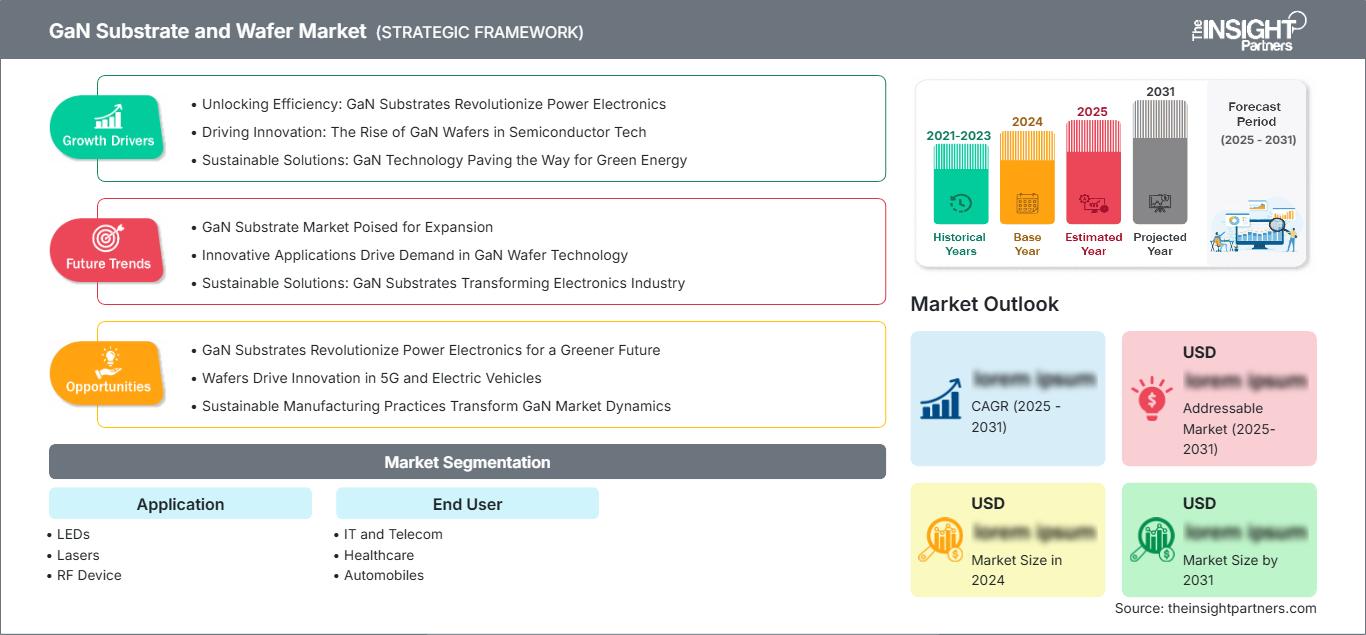
GaN Substrate and Wafer Market: Strategic Insights
Regional Insights
North America GaN Substrate Wafer Market
North America represents 26 to 29% of the Modelled GaN Substrate Wafer Market share in 2025 and grows at a CAGR of 10.8 to 11.6% up to 2034. Defense radars, satellite communications, 5G infrastructure, data center power conversion, and electric mobility drive demand. Government semiconductor incentives, universities, and foundries of radio-frequency circuits help the qualification of substrates, while importing of gallium and specific wafers is the critical vulnerability of the supply chain.
In the region, customers value GaN on silicon carbide for power radio-frequency applications, GaN on silicon for scalable power electronics applications, and native GaN for low-defect laser devices and vertical devices development. Purchasing increasingly includes such factors as traceability, sustainability of supply, compliance with export control regulations, and trusted foundries' requirements. Cooperation of materials producers, epilayers producers, devices makers, and defense laboratories reduces learning curves; however, rigorous reliability tests hinder switching of suppliers.
U.S. GaN Substrate Wafer Market
The U.S. accounts for a modelled 82-86% of the North America demand by 2025 and grows at a 10.9-11.7% CAGR until 2034. This is due to defense electronics purchases, compound semiconductor fabrication sites, telecom equipment design, and power device startups. GaN Systems Inc., and major international players have technical or business operations, while universities and national labs conduct research on substrate characterization, thermal management, and reliability testing.
Application areas of interest include radar systems and satellite modules, fast charging modules, servers, lidar, and automotive power modules. GaN on SiC is important in the case of RF power density, whereas large diameter GaN on silicon plays an important role in switching applications due to low cost concerns. Native GaN technology has been focused on vertical transistors and laser diodes. The demands from customers are increasing and now involve processing capabilities, traceability, wafer specifications, and design assistance.
Europe GaN Substrate Wafer Market
Europe represents a modeled share of 19% to 22% in 2025, growing at 9.8% to 10.6% CAGR till 2034. Germany represents the lead player due to automotive power electronics, industrial drives, MOCVD systems, and research consortiums. United Kingdom provides radio frequency (RF) designs and compound semiconductor ecosystems, whereas France has engineering substrates, aerospace, defense, and semiconductor initiatives.
Italy and Spain bring additional demand from telecommunications, renewables, rail and automotive electronics. Energy efficiency, resilience of supply chain, recyclability of processes, and qualification in automotive and aerospace standards represent priorities for European customers. AIXTRON SE, Soitec S.A., Soitec Belgium N.V. and Compagnie de Saint-Gobain S.A. represent capability players. Joint pilot lines and international research efforts assist in bridging laboratory materials to volume production, despite energy costs and procurement issues.
APAC GaN Substrate Wafer Market
Share modelled for Asia Pacific is 43–47% in 2025, growing at a CAGR of 12.4–13.2% through 2034. Japan is the market leader in high-quality substrate fabrication based on their long-standing crystal growth technology. China will build their business in the manufacture of LED, power electronics, and telecommunication products.
South Korea will combine their display and consumer electronics technologies with investments in compound semiconductors. India will develop their electronics and telecommunication products industry while Australia will contribute their research capabilities, defense applications, and mining power applications to the global compound semiconductors market.
Middle East & Africa GaN Substrate Wafer Market
MEA and Africa grow at 8.9–9.7% CAGR through 2034 according to modelling. The leader is Saudi Arabia on semiconductors, renewables, defense localization and data centers. UAE participates via communications, space, smart infrastructures and funding for advanced technologies; South Africa participates in telecom and R&D.
RoMEA adoption is driven by projects with satellite communications, radars, hard environment power electronics and effective infrastructure. Wafer manufacturing capacity is low, hence imports are critical. Cooperation with international suppliers, universities and technology centers could provide application engineering prior to expensive substrate manufacturing becomes economically viable.
Segmentation Analysis
Application
The Application segment is modelled to expand at an 11.4–12.2% CAGR during 2026–2034. GaN Substrate Wafer Market scope covers established optoelectronics and faster-growing RF and power-device uses. LEDs sustain volume, lasers require low-defect crystals, RF devices favor thermal performance, and transistors benefit from high breakdown fields. Qualification depends on lattice matching, wafer diameter, surface finish, thermal resistance, and compatibility with downstream epitaxy.
- LEDs: Maintain the largest installed demand base through lighting, displays, backlighting, and ultraviolet systems, while efficiency improvement and micro-LED development keep substrate quality strategically important.
- Lasers: Require low-defect, uniform wafers for optical storage, projection, medical equipment, sensing, and industrial processing, making native GaN quality and wavelength consistency decisive.
- RF Device: Demand centers on telecom base stations, radar, satellite links, and electronic warfare, where GaN-on-SiC delivers high power density and heat dissipation.
- Transistors: Represent the fastest-growing application as chargers, data centers, electric vehicles, and industrial converters seek higher switching frequency, compact designs, and reduced power losses.
End User
The End User segment is modelled to grow at an 11.2–12.0% CAGR during 2026–2034. Adoption reflects different qualification priorities across communications, regulated medical systems, vehicles, consumer power products, and defense platforms. IT and telecom emphasize RF and server efficiency; automobiles require lifetime reliability; consumer electronics prioritize cost and size; healthcare values precision; military and defense buyers require trusted supply and extreme-environment performance.
- IT and Telecom: Leads demand through base-station amplifiers, satellite links, data-center power supplies, and network equipment requiring efficient high-frequency operation, thermal control, and reliable wafer availability.
- Healthcare: Uses GaN-enabled lasers, imaging, sterilization, sensing, and compact power systems, with adoption governed by traceability, device reliability, and regulated design cycles.
- Automobiles: Expands through onboard charging, DC-DC conversion, lidar, and power management, where reduced switching losses and smaller thermal systems improve vehicle efficiency.
- Consumer Electronics: Converts wafer performance into compact fast chargers, adapters, displays, and audio products, demanding large-diameter economics, high yield, and rapid product qualification.
- Military and Defense: Prioritizes radar, electronic warfare, secure communications, and space systems, placing exceptional value on RF power density, thermal resilience, provenance, and long-term availability.
Opportunity Snapshot
| Application | Revenue Contribution | Trend Tag | Adoption Stage |
| LEDs | High | Micro LEDs | Mature |
| Lasers | Medium | Low Defects | Scaling |
| RF Device | High | 6G RF | Scaling |
| Transistors | High | Vertical GaN | Emerging |
GaN Substrate Wafer Market Forecasts favor transistors because power conversion combines strong efficiency economics with expanding addressable systems. RF devices remain qualification-intensive and strategically valuable, LEDs provide manufacturing scale, and lasers reward defect control. Capital allocation should prioritize diameter migration, surface consistency, thermal performance, and customer co-development.
GaN Substrate and Wafer Market Growth Drivers and Impact Analysis
5G, 6G, and defense RF systems raise thermal requirements
Telecom densification and defense modernization require amplifiers that sustain output power at high frequencies without excessive cooling. GaN-on-SiC substrates support these designs through strong thermal conductivity and high breakdown fields, enabling compact base-station radios, radar arrays, satellite terminals, and electronic-warfare modules. The substrate impact extends beyond wafer volume: lower defect density, controlled bow, and epi-ready surfaces improve device uniformity and module yield. As networks move toward higher bands and active antenna architectures, each site uses more RF channels. Suppliers that maintain lot consistency and secure SiC and gallium inputs can convert qualification wins into durable production programs, while inferior thermal performance directly restricts power density.
Efficient power conversion expands transistor demand
Data centers, fast chargers, electric vehicles, renewable-energy equipment, and industrial drives are seeking higher switching frequencies and lower conversion losses. GaN transistors can reduce passive-component size and cooling requirements, creating system-level savings that justify premium semiconductor materials. Larger GaN-on-silicon wafers improve fab compatibility and die economics, while native GaN supports vertical architectures for higher voltage. The commercial effect is broader substrate segmentation rather than a single winning platform. Wafer suppliers must align diameter, resistivity, thermal behavior, and surface specifications with device structures. Customers increasingly assess total good-die cost, reliability, and supply assurance, creating opportunities for co-optimized substrate and epitaxy offerings.
Optoelectronics sustain scale and quality investment
LEDs and laser diodes provide an established base for GaN wafer technology, supporting lighting, displays, projection, optical storage, medical systems, sensing, and industrial processing. Micro-LEDs and shorter-wavelength lasers increase sensitivity to crystalline defects, wavelength uniformity, and surface quality. This pushes investment into inspection, polishing, stress control, and native substrates even where conventional sapphire platforms remain cost effective. High-volume optoelectronics also spread fixed processing costs and preserve technical labor that can transfer into power and RF programs. The market impact is a balanced demand profile: mature LED volumes support capacity utilization, while premium laser and display applications reward suppliers capable of tighter defect and uniformity control.
GaN Substrate and Wafer Market Future Trends
Native GaN moves toward larger commercial diameters
GaN Substrate Wafer Market trends point toward four-inch and six-inch native GaN platforms moving from development into selective production. Larger diameters can improve die throughput and compatibility with established fabrication equipment, but crystal uniformity, cracking, bow, and polishing remain difficult. Progress will depend on hydride vapor phase epitaxy, ammonothermal growth, seed reuse, and automated defect mapping. Early adoption should concentrate in laser diodes and vertical power devices, where low dislocation density creates measurable performance value. Suppliers that achieve repeatable quality across the full wafer can command premium positioning before capacity expansion gradually lowers cost.
Engineered thermal substrates reshape RF architectures
Future RF platforms will increasingly combine thin GaN layers with engineered SiC, diamond, or bonded structures to remove heat near active regions. Better thermal pathways can raise output power, extend device life, and reduce cooling hardware in radar and communications modules. Commercialization requires reliable bonding, low interface resistance, scalable wafer handling, and compatibility with existing epitaxy and fabrication flows. Rather than displacing all conventional GaN-on-SiC, engineered substrates will target applications where thermal limits constrain system performance. Partnerships among substrate specialists, equipment vendors, foundries, and module suppliers will be essential for qualification and cost reduction.
GaN Substrate and Wafer Market Opportunities
Build six-inch GaN-on-GaN qualification ecosystems
Investors and suppliers can accelerate six-inch GaN-on-GaN adoption by funding shared pilot lines, standardized defect maps, epitaxy reference processes, and multi-customer reliability programs. Individual device makers often cannot justify the complete learning cost, while substrate producers need predictable demand before scaling crystal growth. Coordinated qualification reduces duplicated testing and clarifies specifications for vertical transistors, laser diodes, and high-voltage devices. Commercial plans should include seed strategy, slicing yield, reclaim pathways, inspection automation, and long-term supply agreements. Successful ecosystems can convert laboratory performance into bankable capacity while establishing regional intellectual property and skilled manufacturing employment.
Localize application engineering near Asian fabs
Asia Pacific combines the largest wafer-consuming base with rapid investment in displays, telecom, vehicles, and power electronics. Suppliers should place application laboratories near major fabs to troubleshoot epitaxy, wafer bow, particles, and device yield in real time. Local teams can also translate customer roadmaps into diameter, doping, resistivity, and surface-finish requirements before global capacity decisions are fixed. The opportunity is not limited to selling wafers: inspection services, substrate reclaim, recipe support, and joint reliability testing create recurring value. Partnerships with Japanese quality leaders, Chinese volume manufacturers, South Korean electronics groups, and Indian emerging fabs diversify exposure.
Recent Developments
- May 2025: Sumitomo electric Industries, Ltd. and Osaka Metropolitan University (Location: Osaka Prefecture; President: Hiroyuki Sakuragi; hereinafter "OMU") have successfully fabricated a gallium nitride transistor (hereinafter "GaN-HEMT") on a 2-inch polycrystalline diamond (PCD) substrate in a joint research project* with the Japan Science and Technology Agency (JST). This technology is an important step toward achieving higher capacity and lower power consumption of core devices in mobile and satellite communications.
- April 2025: Sumitomo Chemical announced that it will participate in PCIM Europe 2025, held in Nuremberg, Germany, from May 6 to 8, 2025. The company will present its latest compound semiconductor technologies, with a particular focus on gallium nitride (GaN) materials for next-generation power devices. At the event, Sumitomo Chemical will showcase GaN substrates and high-purity GaN-on-GaN epitaxial wafers. These materials are expected to play an important role in improving the performance and efficiency of future power semiconductor devices.
- July 2025: Infineon Technologies is making strong progress toward commercial-scale manufacturing of gallium nitride (GaN) power semiconductors using 300-millimeter wafers. The company said its manufacturing roadmap remains on schedule, with initial customer samples expected to be available from the fourth quarter of 2025. The move to 300mm wafers is intended to increase manufacturing efficiency and help reduce the cost of GaN devices. Compared with the commonly used 200mm wafers, a 300mm wafer can accommodate around 2.3 times as many chips, providing significant potential for higher production volumes and improved economies of scale.
Frequently Asked Questions

- Comprehensive Market Sizing and Forecast Analysis
- Detailed Segmentation Analysis
- In-Depth Market Dynamics Assessment
- Regional and Country-Level Insights
- Competitive Landscape and Company Benchmarking
- Strategic Business Intelligence
Recent Reports
Testimonials

The Insight Partners provided valuable market intelligence that supported our global go-to-market strategy. Their team was professional, responsive, and attentive to our feedback, providing thoughtful analysis and helpful methodological clarifications throughout the project.
Junmo Kim Chief Financial Officer (CFO), Enertech Co., Ltd.
The Insight Partners' SCADA System Market report is comprehensive, with valuable insights on current trends and future forecasts. The team was highly professional, responsive, and supportive throughout. We are very satisfied and highly recommend their services.
RAN KEDEM Partner, Reali Technologies LTDs
I requested a report on a very specific software market and the team produced the report in a few days. The information was very relevant and well presented. I then requested some changes and additions to the report. The team was again very responsive and I got the final report in less than a week.
JEAN-HERVE JENN Chairman, Future Analytica
We worked with The Insight Partners for an important market study and forecast. They gave us clear insights into opportunities and risks, which helped shape our plans. Their research was easy to use and based on solid data. It helped us make smart, confident decisions. We highly recommend them.
PIYUSH NAGPAL Sr. Vice President, High Beam Global
The Insight Partners delivered insightful, well-structured market research with strong domain expertise. Their team was professional and responsive throughout. The user-friendly website made accessing industry reports seamless. We highly recommend them for reliable, high-quality research services
YUKIHIKO ADACHI CEO, Deep Blue, LLC.
This is the first time I have purchased a market report from The Insight Partners.While I was unsure at first, I visited their web site and felt more comfortable to take the risk and purchase a market report.I am completely satisfied with the quality of the report and customer service. I had several questions and comments with the initial report, but after a couple of dialogs over email with their analyst I believe I have a report that I can use as input to our strategic planning process.Thank you so much for taking the extra time and making this a positive experience.I will definitely recommend your service to others and you will be my first call when we need further market data.
JOHN SUZUKI President and Chief Executive Officer, Board Director, BK Technologies
I wish to appreciate your support and the professionalism you displayed in the course of attending to my request for information regarding to infectious disease IVD market in Nigeria. I appreciate your patience, your guidance, and the fact that you were willing to offer a discount, which eventually made it possible for us to close a deal. I look forward to engaging The Insight Partners in the future, all thanks to the impression you have created in me as a result of this first encounter.
DR CHIJIOKE ONYIA MANAGING DIRECTOR, PineCrest Healthcare Ltd.Reason to Buy
- Informed Decision-Making
- Understanding Market Dynamics
- Competitive Analysis
- Identifying Emerging Markets
- Customer Insights
- Market Forecasts
- Risk Mitigation
- Boosting Operational Efficiency
- Strategic Planning
- Investment Justification
- Tracking Industry Innovations
- Aligning with Regulatory Trends





 Get Free Sample for