The semiconductor bonding market size is expected to reach US$ 1,076.82 million by 2028, registering at a CAGR of 8.2% from 2022 to 2028, according to a new research study conducted by The Insight Partners.
Increasing Uptake of Die Bonders in Telecommunication Sector to Offer Growth Opportunities for Semiconductor Bonding Market
The growing demand for high-performance optical communication devices boosts 5G deployment and datacenter applications. Further, this supports 5G wireless fronthaul and next-generation Ethernet modules, such as 2x200GbE, 4x100GbE, 400GbE, and CWDM/DWDM transceivers. The demand for high-performance optical devices is generating the need for smaller packaging housing, rapid technology innovation, smaller chips/dies with higher density in the package, higher-volume manufacturing, quick product iterations, and an economical price point. The new requirements are also needed in LiDAR, AR/VR, advanced photonic sensors, MEMS, and highly integrated silicon photonics devices. To manufacture these devices, flexible die bonding solutions with high post-bonding accuracy and great long-term stability are required. Various manufacturers are producing flexible high bonding solutions to meet this requirement. For instance, MRSI-HVM by MRSI Systems is a flexible high-speed die bonder that can achieve <±1.5 µm accuracy. As a result, the company provides the best high volume and high mix manufacturing solutions for 5G and datacenter core devices.
Semiconductor Bonding Market Share - by Geography, 2021
Semiconductor Bonding Market Forecast to 2028 - COVID-19 Impact and Global Analysis By Type (Die Bonder, Wafer Bonder, and Flip Chip Bonder) and Technology (RF Devices, MEMS and Sensors, LED, CMOS Image Sensors, and 3D NAND)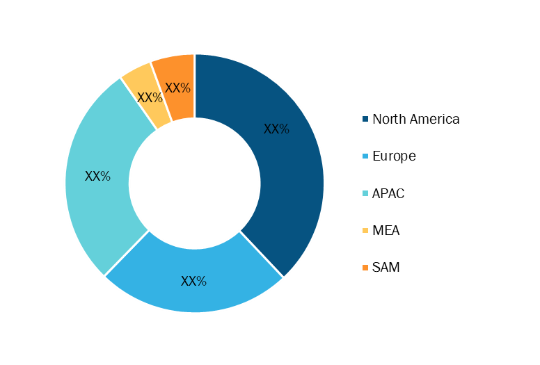
Semiconductor Bonding Market Size, Share | Global Trends 2028
Download Free Sample
The South America semiconductor bonding market size is segmented into Brazil, Argentina, and the Rest of South. The increasing demand for CMOS image sensors in machine vision systems is driving the need for semiconductor bonding equipment. The market growth is attributed to the growing demand for high-quality cameras in smartphones and tablets and the increasing application of image sensors in the medical diagnostic & image sensor, automotive, and other sectors. However, the complex manufacturing process of high-resolution image sensors and higher power consumption in CCD image sensors are hindering the market growth.
Brazil has the biggest telecom industry in South America. In July 2022, the telecommunication industry in Latin America is worth US$ 81 billion, with Brazil being the region's largest market. This will boost the demand for semiconductor bonding technology in the telecommunication industry. Also, the rising demand for 5G in the country will fuel the country’s semiconductor bonding market size. Further, the Brazilian government has invested US$ 45 million to expand the semiconductor industry. Thus, the growing telecommunication industry and government investment will boost the market.
Impact of COVID-19 Pandemic on South America Semiconductor Bonding Market Growth
During the COVID-19 pandemic, the shortage of semiconductor chips, the decline in auto parts production, and the shutdown of international borders affected South American economies such as Brazil and Argentina. In 2020, the COVID-19 pandemic resulted in large-scale adversities in South American economies. The demand and supply sides in the market also experienced a slowdown due to decreased production levels and disrupted international trade activities. However, in 2021, with the relaxation of the lockdown measures, manufacturing businesses, including semiconductor products, resumed operations. The disruptions in logistics systems, shortages of semiconductor chips, and import of bonding products from foreign countries have impacted the South America semiconductor bonding market growth. Thus, South American countries faced a challenge to reestablish economic activities, quicken the manufacturing process of electronics, and make the automotive sector resilient due to supply chain disruption in the import and export of automotive parts. However, the electronics manufacturing and automobile companies in the region are gradually recovering from production and supply chain disruptions. As a result, developing countries such as Brazil, Chile, and Argentina are expected to attract foreign investment in semiconductor bonding manufacturing. Thus, with the upliftment of lockdown restrictions, the market is expected to witness steady growth over the forecast period.
The semiconductor bonding market is segmented on the basis of type, application, and geography. Based on type, the semiconductor bonding market is segmented into die bonder, wafer bonder, and flip chip bonder. Based on application, the market is categorized into RF devices, MEMS and sensors, LED, CMOS image sensors, and 3D NAND. Based on geography, the semiconductor bonding market is primarily segmented into North America, Europe, Asia Pacific (APAC), the Middle East & Africa (MEA), and South America.
Palomar Technologies; Panasonic Corporation; Toray Industries Inc; Kulicke & Soffa Industries, Inc.; HUTEM; DIAS Automation (HK) Ltd; ASMPT Ltd (formerly ASM Pacific Technology Ltd.); EV Group; Yamaha Motor Corporation (Yamaha Robotics Holdings); and WestBond, Inc. are the key semiconductor bonding market players profiled in the study of the semiconductor bonding market. Several other important semiconductor bonding market players were studied and analyzed during the course of this study to get a holistic view of the market and its ecosystem.
Contact Us
Phone: +1-646-491-9876
Email Id: sales@theinsightpartners.com