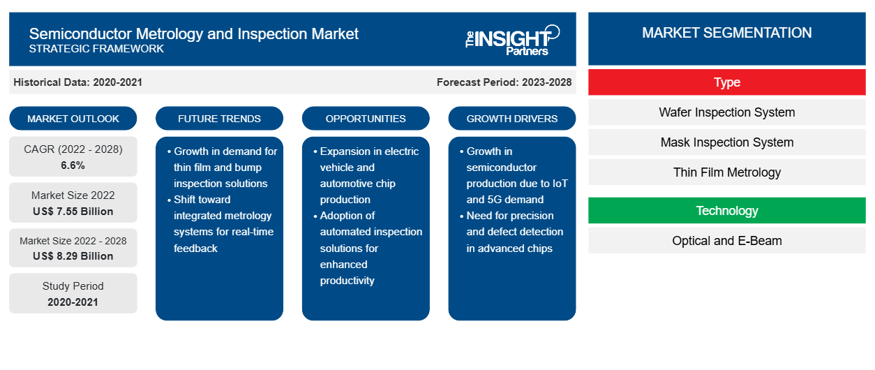
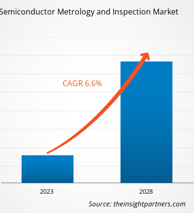
The semiconductor metrology and inspection market is projected to reach US$ 7,553.00 million in 2022 to US$ 8,288.55 million by 2028; it is expected to grow at a CAGR of 6.6% from 2022 to 2028.
The semiconductor industry has been witnessing drastic changes over the years, which have resulted in complex semiconductor manufacturing assembly lines. Growing smart devices application, rising industrial automation, and widespread chips integration in vehicles propel the demand for semiconductors globally. Wafer and mask inspection and other metrology and inspection systems are used in semiconductor inspection in the semiconductor production lines; the systems detect defects and ensure the quality of manufactured semiconductor devices. Owing to the growing demand for semiconductors, semiconductor manufacturers are focused on expanding their manufacturing facilities, leading to growing application of semiconductor metrology and inspection systems. Most players are launching innovative products in the market. For instance, Hitachi High-Tech Corporation introduced the SEM*1 CR7300 high-speed defect inspection in November 2020. The CR7300 is a new review SEM type that will help enhance semiconductor device manufacturing productivity. It is based on electron optics, which allows for the best high-resolution picture acquisition. Simultaneously, new imaging and stage technologies allow for high-speed image acquisition in half the time of traditional methods, reducing total inspection time considerably. In 2022, ASML announced that they have successfully installed a HMI eScan 1100 equipment, the first multiple e-beam (multibeam) wafer inspection system for in-line yield enhancement applications, such as voltage contrast defect inspection and physical defect inspection. The above-mentioned initiatives are expected to create opportunities for semiconductor metrology and inspection market players during the forecast period.
Customize This Report To Suit Your Requirement
You will get customization on any report - free of charge - including parts of this report, or country-level analysis, Excel Data pack, as well as avail great offers and discounts for start-ups & universities
Semiconductor Metrology and Inspection Market: Strategic Insights
- Get Top Key Market Trends of this report.This FREE sample will include data analysis, ranging from market trends to estimates and forecasts.
Impact of COVID-19 Pandemic on Semiconductor Metrology and Inspection Market Players
The continuous growth in the number of novel coronavirus-infected patients compelled government authorities to impose stringent lockdowns across the US and other regions in the first three quarters of 2020. The manufacturing sector witnessed severe losses due to temporary factory shutdowns and low production volumes, which hindered the growth of the automotive, electronics & semiconductor, and retail sectors. The effects of the COVID-19 pandemic shrunk the North America semiconductor metrology and inspection market size in the first three quarters of 2020. In addition, there was a massive disruption in the supply chain across the region due to the lockdown measures, which further triggered a huge backlog of orders, and resulted in the loss of revenue for many large and small enterprises operating in the North America semiconductor metrology and inspection market. However, the market experienced a positive impact since Q4 of 2020. Semiconductor shortage, due to disruptions caused by the pandemic, forced manufacturers to optimize their raw material usage, which led to a higher investment in procuring these equipment, thus boosting the semiconductor metrology and inspection market size This enabled the market players to generate revenues and contribute to the semiconductor metrology and inspection market growth. Nonetheless, the revenue generated in 2020 was slightly less than that generated in 2019, but grew by a substantial amount in 2021. Hence, although the pandemic caused certain disruptions, the semiconductor metrology and inspection player’s businesses were positively impacted due to the pandemic.Semiconductor Metrology and Inspection Market Insights
Advanced packaging (AP) technologies are playing an increasingly critical role across Wafer fabrication, manufacturing, and associated semiconductor processes. With the growing complexity of device architectures and the gain in momentum for heterogeneous integration, AP has emerged as a pivotal enabler of performance enhancement and miniaturization. These developments have significantly influenced the demand landscape for semiconductor metrology and inspection tools, especially within back-end manufacturing environments. Precise control over various processes is essential to ensure the reliability and performance of advanced packaged devices. Unlike front-end semiconductor processes, AP introduces unique challenges for metrology and inspection due to the non-planar, multi-layered nature of advanced packaging structures. Issues such as bump height variation, void detection, misalignment, and nonvisual subsurface defects demand specialized inspection solutions. Moreover, materials diversity—ranging from through-silicon vias (TSVs) to fan-out and chiplet integration—requires highly adaptable and advanced metrology techniques to ensure robust quality control. Inspection and measurement techniques are fundamental to managing yield, identifying defects, and maintaining process uniformity. With the miniaturization of feature sizes and surge in intricacy in interconnect structures, the semiconductor industry witnesses a greater need for metrology systems that offer exceptional accuracy, high sensitivity, and throughput optimization.
The increasing complexity and customization inherent in AP are fueling innovation in inspection technologies, such as 3D optical metrology, X-ray inspection, and infrared imaging systems. These tools are essential for process development and optimization across various AP formats, apart from the prominent role they play in defect detection. As a result, the semiconductor metrology and inspection market is experiencing sustained growth, driven by the ongoing evolution of AP technologies.
The acceleration of AI, 5G, and high-performance computing applications is further amplifying the demand for high-density interconnects and advanced form factors, subsequently boosting reliance on AP. This, in turn, creates robust growth opportunities for metrology and inspection solution providers that can meet the stringent demands of next-generation semiconductor packaging.
Organization Size-Based Insights
The semiconductor metrology and inspection market, by organization size, is segmented into large enterprises and SMEs (Small and Medium Enterprises). The large enterprises segment is expected to register a higher CAGR during the forecast period. Large enterprises are the major end-users of the market. This comprises foundries, such as TSMC and GlobalFoundry, and integrated device manufacturers, such as Intel Corporation and Samsung Corporation. In November 2021, Samsung Corporation announced to build a semiconductor manufacturing unit in Texas due to the increasing requirement for chips for phones and other devices. The company planned to invest US$ 17 billion in building this unit. A significant part of that amount is expected to be utilized for purchasing semiconductor metrology and inspection equipment. Such strategic developments adopted by large enterprises are expected to drive the semiconductor metrology and inspection market growth for this segment during the forecast period.The semiconductor metrology and inspection market is segmented on the basis of type, technology, organization size, and geography.
- Based on type, the market is segmented into wafer inspection system, mask inspection system, thin film metrology, bump inspection, package inspection, lead frame inspection, and probe card inspection.
- Based on technology, the semiconductor metrology and inspection market is segmented into optical and e-beam.
- By organization size, the market is bifurcated into large enterprises and SMEs.
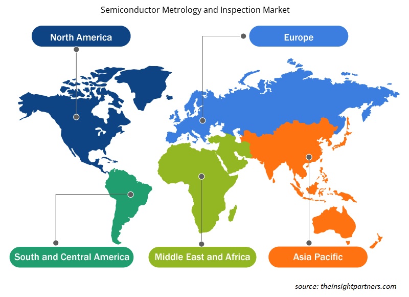
- Based on geography, the semiconductor metrology and inspection market is primarily segmented into North America, Europe, Asia Pacific (APAC), and the rest of the world (ROW).
KLA Corporation; ASML Holding N.V.; Applied Materials, Inc.; Onto Innovation, Inc.; and Hitachi High-Technologies Corporation are among the key market players operating in the market.
Semiconductor Metrology and Inspection Market Regional Insights
The regional trends and factors influencing the Semiconductor Metrology and Inspection Market throughout the forecast period have been thoroughly explained by the analysts at Insight Partners. This section also discusses Semiconductor Metrology and Inspection Market segments and geography across North America, Europe, Asia Pacific, Middle East and Africa, and South and Central America.
- Get the Regional Specific Data for Semiconductor Metrology and Inspection Market
Semiconductor Metrology and Inspection Market Report Scope
| Report Attribute | Details |
|---|---|
| Market size in 2022 | US$ 7.55 Billion |
| Market Size by 2028 | US$ 8.29 Billion |
| Global CAGR (2022 - 2028) | 6.6% |
| Historical Data | 2020-2021 |
| Forecast period | 2023-2028 |
| Segments Covered |
By Type
|
| Regions and Countries Covered | North America
|
| Market leaders and key company profiles |
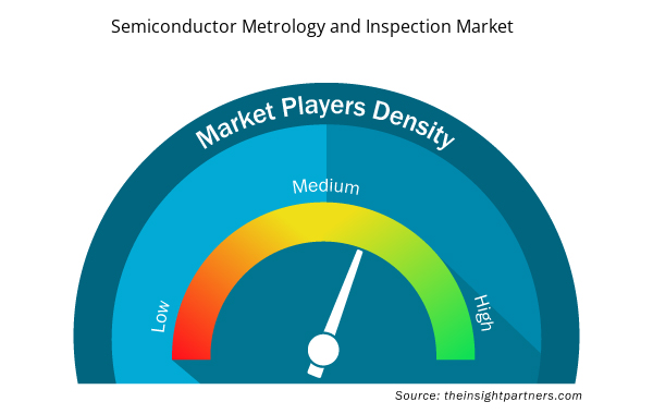
Semiconductor Metrology and Inspection Market Players Density: Understanding Its Impact on Business Dynamics
The Semiconductor Metrology and Inspection Market is growing rapidly, driven by increasing end-user demand due to factors such as evolving consumer preferences, technological advancements, and greater awareness of the product's benefits. As demand rises, businesses are expanding their offerings, innovating to meet consumer needs, and capitalizing on emerging trends, which further fuels market growth.
Market players density refers to the distribution of firms or companies operating within a particular market or industry. It indicates how many competitors (market players) are present in a given market space relative to its size or total market value.
Major Companies operating in the Semiconductor Metrology and Inspection Market are:
- Applied Materials, Inc.
- ASML Holdings N.V.
- Hitachi High-Technologies Corporation
- JEOL, Ltd.
- KLA Corporation
Disclaimer: The companies listed above are not ranked in any particular order.
- Get the Semiconductor Metrology and Inspection Market top key players overview
In the semiconductor metrology and inspection market, the companies are mainly focused on the development of advanced and efficient products.
- In 2022, Lasertec Corporation announced the release of the MATRICS X9ULTRA series, a mask inspection system designed to inspect the photomasks used in extreme ultraviolet (EUV) lithography while their pellicles are not attached.
- In 2020, KLA Corporation announced two new products—the PWG5 wafer geometry system and the Surfscan SP7XP wafer defect inspection system. The new systems are designed to address exceedingly difficult issues in the manufacture of leading-edge memory and logic integrated circuits.
- Historical Analysis (2 Years), Base Year, Forecast (7 Years) with CAGR
- PEST and SWOT Analysis
- Market Size Value / Volume - Global, Regional, Country
- Industry and Competitive Landscape
- Excel Dataset
- Aerosol Paints Market
- Malaria Treatment Market
- Bathroom Vanities Market
- Sweet Potato Market
- Semiconductor Metrology and Inspection Market
- Small Internal Combustion Engine Market
- Fertilizer Additives Market
- Third Party Logistics Market
- Social Employee Recognition System Market
- Microplate Reader Market

Report Coverage
Revenue forecast, Company Analysis, Industry landscape, Growth factors, and Trends

Segment Covered
Type, Technology, and Organization Size

Regional Scope
North America, Europe, Asia Pacific, Middle East & Africa, South & Central America

Country Scope
Canada, China, France, Germany, India, Italy, Japan, MEA, Mexico, Russian Federation, SAM, South Korea, Taiwan, United Kingdom, United States
Frequently Asked Questions
Which country is holding the major market share of APAC semiconductor metrology and inspection market?
China holds the major market share of semiconductor metrology and inspection market in 2022.
Which technology held the largest share in semiconductor metrology and inspection market in 2022?
Optical segment held the largest share in semiconductor metrology and inspection market. Optical semiconductor inspection equipment is one of the most used equipment in semiconductor production line.
What is the future trend in the semiconductor metrology and inspection market?
The increasing use of AI in metrology and inspection systems is one of the major trends anticipated to propel the market growth during the forecast period.
What will be the global market size for semiconductor metrology and inspection market by 2028?
By 2028, the global market size of semiconductor metrology and inspection market will be USD 11,102.53 Million.
Which are the key players holding the major market share of semiconductor metrology and inspection market?
KLA Corporation, ASML Holding N.V., Applied Materials, Inc., Onto Innovation, Inc. and Hitachi High-Technologies Corporation are the five key market players operating in the global semiconductor metrology and inspection market.
What are the driving factors impacting the semiconductor metrology and inspection market?
Rising use of metrology and inspection for advanced packaging processes and surging number of semiconductor applications are major driving factors contributing towards the growth of semiconductor metrology and inspection market.
What is the estimated global market size for the semiconductor metrology and inspection market in 2021?
The global semiconductor metrology and inspection market is expected to be valued at US$ 7,553.00 million in 2022.
Which countries are registering a high growth rate during the forecast period?
The US, Germany, China, and South Korea are registering a high growth rate during the forecast period.
Trends and growth analysis reports related to Electronics and Semiconductor : READ MORE..
The List of Companies - Semiconductor Metrology and Inspection Market
- Applied Materials, Inc.
- ASML Holdings N.V.
- Hitachi High-Technologies Corporation
- JEOL, Ltd.
- KLA Corporation
- Lasertec Corporation
- NOVA Measuring Instruments
- Nikon Metrology N.V.
- Onto Innovation
- Thermofisher Scientific, Inc.
 Get Free Sample For