
Wafer Fabrication Market Size, Trends & Demand by 2034
Coverage: By Type (Oxidation Systems, Diffusion Systems, Photolithography Equipment, Others); Size (50 mm-100 mm, 101 mm-200 mm, Above 200mm); Application (Telecommunications, Medical Devices, Consumer Electronics, Others), and Geography (North America, Europe, Asia Pacific, and South and Central America)
- Status : Data Released
- Report Code : TIPRE00014716
- Category : Electronics and Semiconductor
- No. of Pages : 150
- Available Report Formats :


- Last update date : September 23, 2026


2025 Market Size
US$ 76.63 Bn
Base year value
2034 Forecast
US$ 123.17 Bn
Projected by 2034
CAGR 2026-2034
5.41 %
Growth rate
Addressable Market
US$ 905.86 Bn
(2026-2034)
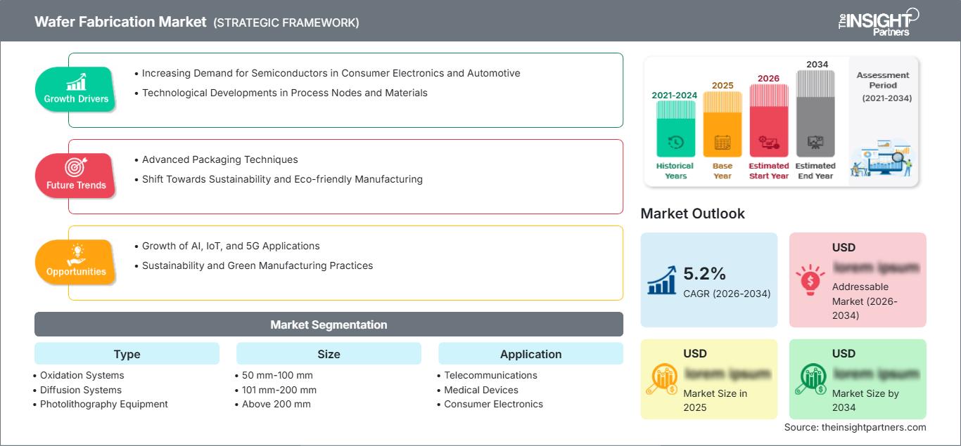
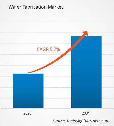
The wafer fabrication market is valued at US$ 76.63 Billion in 2025 and is projected to reach US$ 123.17 Billion by 2034, expanding at a CAGR of 5.41% during 2026–2034. The market encompasses equipment and systems used across critical wafer-processing stages, including oxidation, diffusion, and photolithography, supporting semiconductor production for telecommunications, medical devices, and consumer electronics.
North America is expected to register an estimated CAGR of 5.0–6.0% during 2026–2034, supported by domestic semiconductor capacity expansion, government incentives, and demand for advanced logic and memory devices. Increasing investment in fabrication infrastructure, localized supply chains, and semiconductor research is also strengthening the wafer fabrication market size across the region.
Wafer Fabrication Market Assessment and Insights
- North America: The region is estimated to represent 22–26% share in 2025 and grow at a CAGR of 5.0–6.0% between 2026–2034, supported by fabrication localization, AI infrastructure, and advanced-node investments.
- US: The US is estimated to account for 76–81% of North American demand in 2025 and expand at a CAGR of 5.2–6.2% between 2026–2034 as domestic fabs scale.
- Europe: Europe is estimated at 13–17% share in 2025 and a CAGR of 4.5–5.5% between 2026–2034, led by Germany, France, Italy, and the Netherlands through automotive and industrial semiconductor programs.
- Asia Pacific: Asia Pacific is estimated at 48–54% share in 2025 and a CAGR of 5.7–6.7% between 2026–2034, led by Taiwan, China, Japan, South Korea, and India through concentrated fabrication ecosystems.
- Largest Segment: Photolithography Equipment is estimated to hold a 38–43% market share in 2025 and expand at a 5.8–6.8% CAGR during 2026–2034, reflecting its critical patterning role.
- High Growth Segment: Above 200 mm wafers are estimated at a 58–63% market share in 2025 and a 6.0–7.0% CAGR during 2026–2034, supported by advanced-node manufacturing.
- Key companies analyzed in detail: Applied Materials, Inc.; Electronics Industry Public Company Limited; Hitachi High-Tech Corporation; Lam Research Corporation; Intel Corporation; SCREEN Semiconductor Solutions Co., Ltd.; Nikon Corporation; Soitec; Taiwan Semiconductor Manufacturing Company Limited; Tokyo Electron Limited.
Source: The Insight Partners' analysis based on proprietary research, government publications, company annual reports, investor presentations, industry databases, and expert interviews.
The wafer fabrication market has evolved from equipment optimized primarily for planar transistor structures toward highly integrated process platforms supporting advanced nodes, heterogeneous integration, and increasingly complex wafer architectures. Bigger wafers provide better throughput, whereas smaller process windows result in more stringent demands on lithography accuracy, thermal stability, contamination controls, and process uniformity.
Over the course of the forecast period, investments will expand beyond traditional Asian production hubs to the United States, Europe, and certain emerging production facilities. Semiconductor industrial policies, supply-chain resilience objectives, and rising demand from artificial intelligence, high-performance computing, automotive electronics, and connectivity applications should sustain equipment deployment while encouraging geographically distributed production, contributing to the overall Wafer Fabrication Market share.
Wafer Fabrication Market Report Scope
| Report Attribute | Details |
|---|---|
| Market size in 2025 | US$ 76.63 Billion |
| Market Size by 2034 | US$ 123.17 Billion |
| Global CAGR (2026 - 2034) | 5.41% |
| Historical Data | 2021-2024 |
| Forecast period | 2026-2034 |
Wafer Fabrication Market Analysis
Demand is increasingly shaped by semiconductor complexity rather than unit volumes alone. AI accelerators, high-bandwidth memory, advanced processors, connectivity chips, and automotive semiconductors require tighter process control and greater equipment intensity. SEMI projected global wafer fab equipment sales of US$115.7 billion in 2025, with 11.0% growth, while foundry and logic equipment demand remained particularly strong.
The wafer fabrication market growth is supported by an interconnected ecosystem involving equipment manufacturers, wafer suppliers, foundries, integrated device manufacturers, chemical suppliers, mask providers, and process-control specialists. Supply dynamics continue to revolve around technologically advanced equipment categories, resulting in lengthy qualification processes and high switching costs for semiconductor firms looking to achieve reliable yields.
The rivalry level among the semiconductor equipment suppliers is high among those that have differentiated process technologies, large installed bases, and co-development capabilities. These players include Applied Materials, Inc., Lam Research Corporation, and Tokyo Electron Limited, whereas Nikon Corporation and SCREEN Semiconductor Solutions Co., Ltd. provide specialized lithography and cleaning services. Hitachi High-Tech Corporation adds process-control and inspection capabilities, according to the Wafer Fabrication Market report.
There have been emerging investment plans whereby capacity expansion, localization, and technology partnerships are involved. This can be seen in Taiwan Semiconductor Manufacturing Company Limited's plans to expand through capacity building in Taiwan, America, Japan, and Europe. Also, there is continuous development of local manufacturing by Intel Corporation. In addition, there is provision of wafer materials by Soitec, and a technology partnership in the region from Electronics Industry Public Company Limited.
● REPORT CUSTOMIZATION
Tailor This Report To Align With Your Specific Business Requirements
This report can be customized to align precisely with your business objectives, scope, and target markets. Customization options include tailored segmentation, geography, competitive analysis, and strategic insights to support informed decision-making.
Customize This Report →WHAT YOU CAN ADJUST
- ● Segmentations
- ● Geography
- ● Competitive Analysis
- ● Language Preferences
Wafer Fabrication Market: Strategic Insights
Regional Insights
North America wafer fabrication market
North America is estimated to represent 22–26% share in 2025 and expand at a 5.0–6.0% CAGR during 2026–2034. The United States is the dominant source of regional demand for semiconductors, with the expansion of capacity in the country for advanced logic, memory, and specialty chips. There are initiatives being taken by the government to reduce reliance on foreign capacity in favor of local capacity, which increases demand for front-end equipment and fabrication.
The region has the advantage of having strong players in terms of equipment suppliers, semiconductor design, research organizations, and technology firms. Arizona and Texas have emerged as manufacturing regions, while California remains the stronghold of equipment innovation and semiconductor research. AI computing is driving the demand for high equipment intensity due to leading-edge nodes and high-performance computing.
U.S. wafer fabrication Market
The US is estimated to represent 76–81% of North American wafer fabrication market demand in 2025, with a 5.2–6.2% CAGR during 2026–2034. The need for equipment is being driven further by new fabrication plant construction, investments into advanced packaging, and initiatives to create robust semiconductor supply chains. Top vendors have large operational and service footprints for their local fabs.
Applications span from AI accelerators to telecommunication processors, medical electronics, automotive semiconductors, and consumer products. The Taiwan Semiconductor Manufacturing Company Limited stated that it has several fabs and advanced packaging plants within the Arizona expansion, while Tokyo Electron Limited has 19 sites and around 3,400 employees in the US.
Europe wafer fabrication Market
Europe is estimated to hold 13–17% share of the wafer fabrication market in 2025 and grow at a 4.5–5.5% CAGR through 2034. Germany is the top regional manufacturing hub because of the demands of semiconductors for the automotive industry and new foundries. The UK participates in research and design, while France, Italy, and Spain contribute to specialty and automotive semiconductor markets, along with power and industrial semiconductors. Germany will continue to be the leading country because of its manufacturing depth and automotive focus.
Germany is seeing investments in advanced fabrication related to automotive and industrial uses, such as that of Taiwan Semiconductor Manufacturing Company Limited's new Dresden fab. The UK focuses on semiconductor research, compound materials, and technology. France remains strong in automotive and industrial electronics, while Italy offers support for power semiconductors and automotive production. Spain is developing its own semiconductor manufacturing capabilities through technology investment and development.
APAC wafer fabrication Market
APAC is estimated to command 48–54% share of the wafer fabrication market in 2025 and expand at a 5.7–6.7% CAGR through 2034. Taiwan is still the leading producer country, then come China, Japan, South Korea, India, and Australia. APAC is rich with a semiconductor ecosystem, proven suppliers, large-scale foundries, and electronics manufacturing.
Taiwan and South Korea remain key players in advanced logic and memory manufacture, and Japan stands out for its excellence in equipment, materials, and specialty manufacturing. China is continuously building domestic semiconductor capacities, India is growing its fabrication infrastructure and promoting localization of electronics, and Australia stays small but provides research and specialized semiconductor production. APAC's regional policies and AI capacities demand would preserve its leadership.
Middle East & Africa wafer fabrication Market
The Middle East and Africa wafer fabrication market is projected to expand at a 3.8–4.8% CAGR through 2034, supported by technology localization, electronics demand, and infrastructure modernization. Saudi Arabia and the UAE are becoming centers of investments and technological development, while South Africa continues to contribute with its existing industrial and research base. The UAE is projected to be at the forefront of investment initiatives in the region related to semiconductors.
Saudi Arabia is working on its advanced technologies and industrial diversification efforts, while the UAE is building its digital and high technology investment ecosystem. South Africa continues to be important because of electronics, research, and industrial applications. RoMEA demand is relatively fragmented; however, there could be some new opportunities related to energy, telecommunication infrastructure, and smart city developments that would require semiconductors.
Segmentation Analysis
Type
Type is segmented into Oxidation Systems, Diffusion Systems, and Photolithography Equipment. Photolithography Equipment is estimated to expand at a 5.8–6.8% CAGR during 2026–2034 and represents the largest type category because pattern definition remains fundamental to semiconductor scaling. Oxidation and diffusion systems remain essential for controlled thermal processing and dopant-related manufacturing steps, as highlighted in the Wafer Fabrication Market forecast.
- Oxidation Systems: These systems support controlled oxide formation and remain strategically important for device isolation, dielectric structures, and specialty semiconductor manufacturing. Demand depends on process architecture, thermal uniformity, and high-volume production requirements.
- Diffusion Systems: Diffusion systems remain relevant for dopant introduction and thermal treatment across mature and specialty nodes. Their value is reinforced by reliable batch processing, repeatability, and compatibility with established fabrication workflows.
- Photolithography Equipment: Photolithography equipment occupies the most strategically important position because circuit pattern transfer determines feature resolution, overlay accuracy, and process scalability across increasingly sophisticated semiconductor generations.
Size
Size comprises 50 mm–100 mm, 101 mm–200 mm, and Above 200 mm. Above 200 mm wafers are estimated to grow at a 6.0–7.0% CAGR during 2026–2034 and remain the largest category because 300 mm production provides substantial throughput and productivity advantages for high-volume semiconductor manufacturing, reflecting key Wafer Fabrication Market trends.
- 50 mm-100 mm: Smaller wafers remain relevant for research, specialty devices, sensors, and selected compound semiconductor applications. Their strategic role is linked to low-volume production and processes that do not justify larger wafer platforms.
- 101 mm-200 mm: Mid-sized wafers continue serving mature-node, analog, power, and specialty semiconductor manufacturing. Demand remains supported by established fabs where equipment longevity and process stability are more important than maximum wafer throughput.
- Above 200 mm: Large wafers dominate advanced and high-volume production because they improve die output per process cycle. Their adoption increases equipment utilization requirements and reinforces investment in high-throughput fabrication platforms.
Application
Application includes Telecommunications, Medical Devices, and Consumer Electronics. Application demand is supported by increasing semiconductor content, connectivity requirements, device miniaturization, and reliability expectations. Telecommunications provides recurring demand from networking infrastructure, medical devices require highly controlled semiconductor performance, and consumer electronics contribute significant volume across processors, sensors, displays, and connectivity components.
- Telecommunications: Semiconductor demand is linked to network infrastructure, wireless connectivity, optical communications, and data-center expansion. Increasing bandwidth requirements encourage investment in higher-performance components and advanced fabrication processes.
- Medical Devices: Medical applications prioritize reliability, low power consumption, sensing accuracy, and long product lifecycles. Semiconductor requirements span imaging, monitoring, diagnostics, wearable devices, and implantable or portable equipment.
- Consumer Electronics: Consumer electronics remain a high-volume application supported by smartphones, personal computers, wearables, connected appliances, and entertainment devices. Product refresh cycles create recurring demand for increasingly capable semiconductor components.
Opportunity Snapshot
| Application | Revenue Contribution | Trend Tag | Adoption Stage |
| Telecommunications | High | Network Upgrades | Mature |
| Medical Devices | Medium | Digital Diagnostics | Scaling |
| Consumer Electronics | High | AI Devices | Mature |
Wafer Fabrication Market Growth Drivers and Impact Analysis
AI Computing Is Increasing Semiconductor Process Intensity
Advanced equipment needs for AI accelerators and supercomputers include advanced processing chips, memory, networking, and more advanced packaging architectures. Equipment intensity is affected since more intensive geometry will call for more steps, such as deposition, etch, clean, lithography, and process control. According to SEMI's forecasts for 2025, wafer fab equipment sales would amount to US$115.7 billion, with spending on leading-edge logic and high bandwidth memory associated with AI being a key driver. The effects are not limited to leading-edge fabs, given that AI server needs include power management, connectivity, storage, and other semiconductor components. Suppliers of equipment that offer a wide range of processes can take advantage of that demand throughout various production processes.
Government Incentives Are Reshaping Semiconductor Manufacturing Geography
Strategic policies of the semiconductor industry are urging manufacturing firms to diversify their production operations in North America, Europe, and Asia instead of having all their capabilities within existing sites. Such policies will lower the cost and capital requirements of building new fabs while adding strategic flexibility to the country and the manufacturers. The Taiwanese company named Taiwan Semiconductor Manufacturing Company Limited, exemplifies the extent of such a trend in the semiconductor industry through its plan to have new fabs and packaging facilities, along with the establishment of a research center in the USA. The diversification of operations by suppliers provides them with more flexibility in terms of dependency on individual customers or manufacturing centers.
Advanced Process Nodes Are Raising Requirements for Precision Equipment
Reduced feature size makes the system more susceptible to contaminants, overlay, temperature changes, variations in thickness, and process variations. In an attempt to migrate towards advanced logic technologies, the equipment is expected to have better precision while maintaining commercial viability. TSMC stated that 74% of its wafer revenue in 2025 for advanced technology, which includes 7 nm and below, was generated from the 69% it had in 2024. This calls for more complex technologies in patterning, deposition, etching, cleaning, inspection, and metrology. Equipment companies that can prove process window stability and fast yield learning enjoy an advantage during fab start-ups. The requirements lead to increased qualification challenges, which further add to the competitive strength of incumbents with a good customer and equipment base.
Wafer Fabrication Market Future Trends
Equipment Intelligence Will Move Toward Closed-Loop Process Optimization
Advanced fab facilities are expected to feature more automation, sensors, predictive analytics, and software-controlled process tuning. In addition to being a standalone monitoring function for equipment, advanced fabs will link process monitoring directly with the manufacturing execution system and yield management system. This can lead to less unscheduled downtime, early detection of drifts, and better consistency between different process tools and/or production lines. Digital twin and machine learning models could be used to perform recipe optimization prior to implementation in the real process environment. The business case depends not on the functionality of software, but on its effect on wafer yield, equipment uptime, and energy consumption. Suppliers who combine their hardware experience and process analytics could benefit in the market of advanced fabs.
Regional Fab Networks Will Become More Interconnected
It seems that the semiconductor manufacturing industry is going to experience geographical diversification coupled with technological interdependence. The major companies will maintain their key capacity at advanced nodes in existing centers while establishing regional facilities for special customers, automotive applications, mature node semiconductors, and redundancy purposes. TSMC operates its production facilities in Taiwan, China, Japan, the USA, and is working on building them in Germany. Such a setup requires standardizing the manufacturing processes, equipment services, spare parts, and engineering support throughout continents. There will be more need for equipment makers to have a locally based technical staff and resilient logistics, along with the development of sophisticated products.
Wafer Fabrication Market Opportunities
Localized Equipment Service and Process Support
An increased presence of fab facilities that operate outside of traditional semiconductor centers allows equipment providers to develop regional support infrastructures for new fabs. Availability of equipment during the ramping stage is critical since the downtime can result in a delayed qualification schedule and late delivery to customers. Local engineering support, spare parts centers, remote diagnostics, training and application labs can reduce the time required to solve the problem and create a solid long-term business relationship. Such a situation appears to be most relevant for the USA and Europe, where new fabs are being developed together with the existing Asian semiconductor manufacturing base. Another possibility is to utilize regional technology centers to tailor the equipment to local processes. The biggest opportunities for equipment providers appear to exist where both service and application engineering are provided by equipment vendors.
Advanced Wafer Platforms for Specialized Semiconductor Applications
The manufacture of specialty semiconductors offers an additional avenue other than the most cutting-edge logic nodes. There are power devices, sensors, medical devices, telecommunication ICs, automotive electronics, and compound semiconductors that need equipment designed specifically for different materials, wafers and processes. Equipment providers can serve these sectors using modular systems with the capability for varied process recipes and chamber designs as well as economical manufacture at different volumes. Diversification in demand will help reduce dependence on the cyclical spending patterns of a few advanced foundries. Novel material systems will also present chances for equipment that can handle new material systems and thermal conditions. Providers who create early partnerships with specialty device makers will have the chance to be involved in qualification processes even before full-scale production starts.
Frequently Asked Questions

- Comprehensive Market Sizing and Forecast Analysis
- Detailed Segmentation Analysis
- In-Depth Market Dynamics Assessment
- Regional and Country-Level Insights
- Competitive Landscape and Company Benchmarking
- Strategic Business Intelligence
Recent Reports
Testimonials

The Insight Partners provided valuable market intelligence that supported our global go-to-market strategy. Their team was professional, responsive, and attentive to our feedback, providing thoughtful analysis and helpful methodological clarifications throughout the project.
Junmo Kim Chief Financial Officer (CFO), Enertech Co., Ltd.
The Insight Partners' SCADA System Market report is comprehensive, with valuable insights on current trends and future forecasts. The team was highly professional, responsive, and supportive throughout. We are very satisfied and highly recommend their services.
RAN KEDEM Partner, Reali Technologies LTDs
I requested a report on a very specific software market and the team produced the report in a few days. The information was very relevant and well presented. I then requested some changes and additions to the report. The team was again very responsive and I got the final report in less than a week.
JEAN-HERVE JENN Chairman, Future Analytica
We worked with The Insight Partners for an important market study and forecast. They gave us clear insights into opportunities and risks, which helped shape our plans. Their research was easy to use and based on solid data. It helped us make smart, confident decisions. We highly recommend them.
PIYUSH NAGPAL Sr. Vice President, High Beam Global
The Insight Partners delivered insightful, well-structured market research with strong domain expertise. Their team was professional and responsive throughout. The user-friendly website made accessing industry reports seamless. We highly recommend them for reliable, high-quality research services
YUKIHIKO ADACHI CEO, Deep Blue, LLC.
This is the first time I have purchased a market report from The Insight Partners.While I was unsure at first, I visited their web site and felt more comfortable to take the risk and purchase a market report.I am completely satisfied with the quality of the report and customer service. I had several questions and comments with the initial report, but after a couple of dialogs over email with their analyst I believe I have a report that I can use as input to our strategic planning process.Thank you so much for taking the extra time and making this a positive experience.I will definitely recommend your service to others and you will be my first call when we need further market data.
JOHN SUZUKI President and Chief Executive Officer, Board Director, BK Technologies
I wish to appreciate your support and the professionalism you displayed in the course of attending to my request for information regarding to infectious disease IVD market in Nigeria. I appreciate your patience, your guidance, and the fact that you were willing to offer a discount, which eventually made it possible for us to close a deal. I look forward to engaging The Insight Partners in the future, all thanks to the impression you have created in me as a result of this first encounter.
DR CHIJIOKE ONYIA MANAGING DIRECTOR, PineCrest Healthcare Ltd.Reason to Buy
- Informed Decision-Making
- Understanding Market Dynamics
- Competitive Analysis
- Identifying Emerging Markets
- Customer Insights
- Market Forecasts
- Risk Mitigation
- Boosting Operational Efficiency
- Strategic Planning
- Investment Justification
- Tracking Industry Innovations
- Aligning with Regulatory Trends





 Get Free Sample for