
Thin Wafer Processing and Dicing Equipment Market Trends, Size & Growth by 2034
Coverage: By Equipment Type (Dicing Equipment, Blade Dicing, Laser Ablation, Stealth Dicing, Plasma Dicing); Application (Memory and Logic, LED, MEMS Devices, Power Devices, CMOS Image Sensors, RFID, Others) , and Geography (North America, Europe, Asia Pacific, and South and Central America)
- Status : Data Released
- Report Code : TIPRE00026913
- Category : Electronics and Semiconductor
- No. of Pages : 150
- Available Report Formats :


- Last update date : May 26, 2026


2025 Market Size
US$ 707.44 Mn
Base year value
2034 Forecast
US$ 983.27 Mn
Projected by 2034
CAGR 2026-2034
3.73 %
Growth rate
Addressable Market
US$ 7,680.57 Mn
(2026-2034)
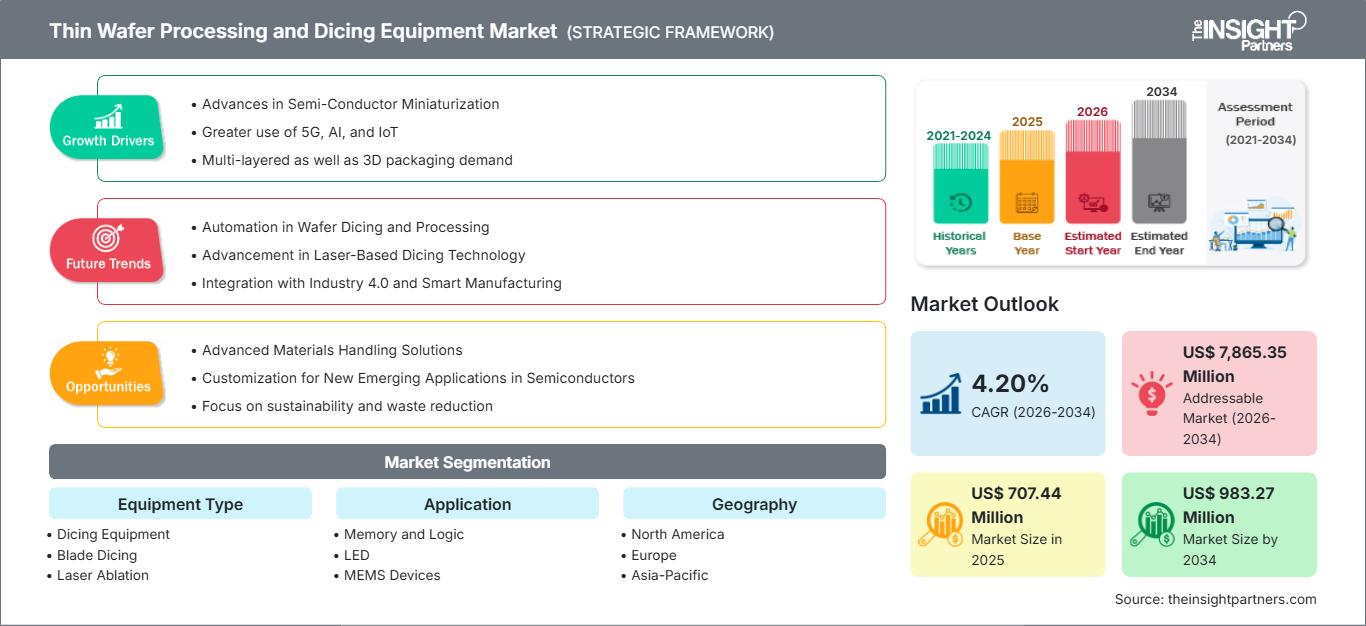
The Thin Wafer Processing and Dicing Equipment market was valued at US$ 707.44 million in 2025 and is expected to reach US$ 983.27 million by 2034; it is estimated to record a CAGR of 3.73% during 2026-2034.
The Thin Wafer Processing and Dicing Equipment Market is categorized by equipment type into the following subsegments: Dicing Equipment, Blade Dicing, Laser Ablation, Stealth Dicing, and Plasma Dicing. It further presents an analysis based on applications, i.e., Memory and Logic, LED, MEMS Devices, Power Devices, CMOS Image Sensors, RFID, and Others. The global analysis is broken down at the regional level and major countries. The market evaluation is presented in US$ for the above segmental analysis.
Purpose of the Report
The report Thin Wafer Processing and Dicing Equipment Market by The Insight Partners aims to describe the present landscape and future growth, top driving factors, challenges, and opportunities. This will provide insights to various business stakeholders, such as:
- Technology Providers/Manufacturers: To understand the evolving market dynamics and know the potential growth opportunities, enabling them to make informed strategic decisions.
- Investors: To conduct a comprehensive trend analysis regarding the market growth rate, market financial projections, and opportunities that exist across the value chain.
- Regulatory bodies: To regulate policies and police activities in the market with the aim of minimizing abuse, preserving investor trust and confidence, and upholding the integrity and stability of the market.
Thin Wafer Processing and Dicing Equipment Market Segmentation Equipment Type
- Dicing Equipment
- Blade Dicing
- Laser Ablation
- Stealth Dicing
- Plasma Dicing
Application
- Memory and Logic
- LED
- MEMS Devices
- Power Devices
- CMOS Image Sensors
- RFID
- Others
Market Assessment and Insights
- Global market for Thin Wafer Processing and Dicing Equipment was valued at US$ 707.44 Million in 2025
- Annual market size is expected to reach US$ 983.27 Million by 2034
- Total addressable market (TAM) during 2026-2034 is projected to reach approximately US$ 7,865.35 Million
- Market is anticipated to register a CAGR of 4.2% during the forecast period
- The United States represents a key market, supported by Advances in Semi-Conductor Miniaturization, Greater use of 5G, AI, and IoT, Multi-layered as well as 3D packaging demand, as well as evolving industry dynamics
- Market analysis covers North America, Europe, Asia-Pacific, South and Central America, Middle East and Africa, with growth evaluated across the forecast period
- Market opportunities such as Advanced Materials Handling Solutions, Customization for New Emerging Applications in Semiconductors, Focus on sustainability and waste reduction are expected to influence market dynamics and addressable market
- Report profiles industry participants, including Suzhou Delphi Laser Co. Ltd, SPTS Technologies Limited, Plasma-Therm LLC, Han's Laser Technology Industry Group Co. Ltd., ASM Laser Separation International (ALSI) B.V., Disco Corporation, Tokyo Seimitsu Co, Ltd. (Accretech), Neon Tech Co. Ltd., Nippon Pulse Motor Taiwan (NPMT), Panasonic Corporation, while analyzing competitive strategies and innovation developments
-
Source: The Insight Partners' analysis based on proprietary research, government publications, company annual reports, investor presentations, industry databases, and expert interviews.
● REPORT CUSTOMIZATION
Tailor This Report To Align With Your Specific Business Requirements
This report can be customized to align precisely with your business objectives, scope, and target markets. Customization options include tailored segmentation, geography, competitive analysis, and strategic insights to support informed decision-making.
Customize This Report →WHAT YOU CAN ADJUST
- ● Segmentations
- ● Geography
- ● Competitive Analysis
- ● Language Preferences
Thin Wafer Processing and Dicing Equipment Market: Strategic Insights
-
Get Top Key Market Trends of this report.This FREE sample will include data analysis, ranging from market trends to estimates and forecasts.
Thin Wafer Processing and Dicing Equipment Market Growth Drivers
- Advances in Semi-Conductor Miniaturization: The driving nature of miniaturization within the semiconductor industry, particularly the effort toward having even smaller and yet more powerful chips, implies the demand for thin wafer processing and dicing equipment. In such equipment, ultra-thin wafers are cut with high accuracy.
- Greater use of 5G, AI, and IoT: The increasing adoption of cutting-edge technologies such as 5G, AI, and IoT devices is generating an insatiable demand for miniaturized, ultra-thin, high-performance semiconductor devices. Thin wafer processing and dicing equipment play a critical role in the production of smaller high-end chips for these applications.
- Multi-layered as well as 3D packaging demand: The market has become focused towards the semiconductor device using more and more multi-layered as well as 3D packaging technologies. The thin wafer processing and dicing equipment hold a prime position in providing precision to such advanced packaging solutions.
Thin Wafer Processing and Dicing Equipment Market Future Trends
- Automation in Wafer Dicing and Processing: It is a significant trend being seen in wafer processing and dicing. The automated systems ensure faster processing, make fewer defects, and enhanced throughput, thereby helping to improve the demand for semiconductors in every application of smartphones and automotive electronics.
- Advancement in Laser-Based Dicing Technology: There is an increase in laser-based dicing technologies that give non-mechanical cutting solutions for ultra-thin wafers with precision and workability with complex materials without stress or damages caused.
- Integration with Industry 4.0 and Smart Manufacturing: Integration of wafer processing equipment with Industry 4.0 technologies such as IoT, AI, and data analytics enables smart and efficient manufacturing processes in real-time with predictive maintenance and process optimization.
Thin Wafer Processing and Dicing Equipment Market Opportunities
- Advanced Materials Handling Solutions: With smaller and thinner to almost delicates a new opportunity was developed to create advanced material handling solutions for safe processing and transportation of wafers in the manufacturing process.
- Customization for New Emerging Applications in Semiconductors: Thin wafer processing and dicing equipment manufacturers can design solutions for the new application fields of quantum computing, flexible electronics, and even wearable devices that demand special wafer handling capabilities.
- Focus on sustainability and waste reduction: This is an opportunity to develop wafer processing and dicing equipment minimizing material loss and energy consumption that will support more sustainable practices in manufacturing. Focusing on Sustainability and Waste Reduction: the pressure increase upon the semiconductor industry to reduce waste and develop higher energy efficiency would not pass without its opportunities.
Thin Wafer Processing and Dicing Equipment Market Report Scope
| Report Attribute | Details |
|---|---|
| Market size in 2025 | US$ 707.44 Million |
| Market Size by 2034 | US$ 983.27 Million |
| Global CAGR (2026 - 2034) | 3.73% |
| Historical Data | 2021-2024 |
| Forecast period | 2026-2034 |
| Segments Covered |
By Equipment Type
|
| Regions and Countries Covered |
North America
|
| Market leaders and key company profiles |
|
Thin Wafer Processing and Dicing Equipment Market Players Density: Understanding Its Impact on Business Dynamics
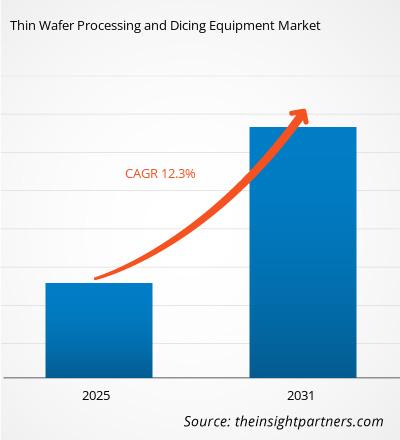
The Thin Wafer Processing and Dicing Equipment Market is growing rapidly, driven by increasing end-user demand due to factors such as evolving consumer preferences, technological advancements, and greater awareness of the product's benefits. As demand rises, businesses are expanding their offerings, innovating to meet consumer needs, and capitalizing on emerging trends, which further fuels market growth.
Key Selling Points
- Comprehensive Coverage: The report comprehensively covers the analysis of products, services, types, and end users of the Thin Wafer Processing and Dicing Equipment Market, providing a holistic landscape.
- Expert Analysis: The report is compiled based on the in-depth understanding of industry experts and analysts.
- Up-to-date Information: The report assures business relevance due to its coverage of recent information and data trends.
- Customization Options: This report can be customized to cater to specific client requirements and suit the business strategies aptly.
The research report on the Thin Wafer Processing and Dicing Equipment Market can, therefore, help spearhead the trail of decoding and understanding the industry scenario and growth prospects. Although there can be a few valid concerns, the overall benefits of this report tend to outweigh the disadvantages.
Frequently Asked Questions

- Comprehensive Market Sizing and Forecast Analysis
- Detailed Segmentation Analysis
- In-Depth Market Dynamics Assessment
- Regional and Country-Level Insights
- Competitive Landscape and Company Benchmarking
- Strategic Business Intelligence
Recent Reports
Testimonials

The Insight Partners' SCADA System Market report is comprehensive, with valuable insights on current trends and future forecasts. The team was highly professional, responsive, and supportive throughout. We are very satisfied and highly recommend their services.
RAN KEDEM Partner, Reali Technologies LTDs
I requested a report on a very specific software market and the team produced the report in a few days. The information was very relevant and well presented. I then requested some changes and additions to the report. The team was again very responsive and I got the final report in less than a week.
JEAN-HERVE JENN Chairman, Future Analytica
We worked with The Insight Partners for an important market study and forecast. They gave us clear insights into opportunities and risks, which helped shape our plans. Their research was easy to use and based on solid data. It helped us make smart, confident decisions. We highly recommend them.
PIYUSH NAGPAL Sr. Vice President, High Beam Global
The Insight Partners delivered insightful, well-structured market research with strong domain expertise. Their team was professional and responsive throughout. The user-friendly website made accessing industry reports seamless. We highly recommend them for reliable, high-quality research services
YUKIHIKO ADACHI CEO, Deep Blue, LLC.
This is the first time I have purchased a market report from The Insight Partners.While I was unsure at first, I visited their web site and felt more comfortable to take the risk and purchase a market report.I am completely satisfied with the quality of the report and customer service. I had several questions and comments with the initial report, but after a couple of dialogs over email with their analyst I believe I have a report that I can use as input to our strategic planning process.Thank you so much for taking the extra time and making this a positive experience.I will definitely recommend your service to others and you will be my first call when we need further market data.
JOHN SUZUKI President and Chief Executive Officer, Board Director, BK Technologies
I wish to appreciate your support and the professionalism you displayed in the course of attending to my request for information regarding to infectious disease IVD market in Nigeria. I appreciate your patience, your guidance, and the fact that you were willing to offer a discount, which eventually made it possible for us to close a deal. I look forward to engaging The Insight Partners in the future, all thanks to the impression you have created in me as a result of this first encounter.
DR CHIJIOKE ONYIA MANAGING DIRECTOR, PineCrest Healthcare Ltd.Reason to Buy
- Informed Decision-Making
- Understanding Market Dynamics
- Competitive Analysis
- Identifying Emerging Markets
- Customer Insights
- Market Forecasts
- Risk Mitigation
- Boosting Operational Efficiency
- Strategic Planning
- Investment Justification
- Tracking Industry Innovations
- Aligning with Regulatory Trends





 Get Free Sample for