
Electronic Packaging Market Size, Growth & Trends by 2034
Coverage: By Product Type (Corrugated Boxes, Paperboard Boxes, Thermoformed Trays, Bags and Pouches, Blister Packs and Clamshells, Protective Packaging, Others); Application Type (Mobile Phones, Computers, Laptops and Tablets, Desktops and Servers, TVs, DTH and Set-Top Boxes, Music Systems, Printers, Scanners and Photocopy Machines, Game Consoles and Toys, Camcorders and Cameras, Electronic Wearable, Digital Media Adapters (DMRs), Others); Material Type (Plastic, PE, PP, PVC, PA, PET, PS, Paper and Paperboard, Others) , and Geography (North America, Europe, Asia Pacific, and South and Central America)
- Status : Data Released
- Report Code : TIPRE00009302
- Category : Electronics and Semiconductor
- No. of Pages : 150
- Available Report Formats :


- Last update date : August 12, 2026


2025 Market Size
US$ 69.71 Bn
Base year value
2034 Forecast
US$ 115.83 Bn
Projected by 2034
CAGR 2026-2034
5.80 %
Growth rate
Addressable Market
US$ 840.54 Bn
(2026-2034)
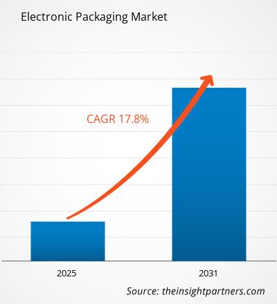
The Electronic Packaging Market reached a value of US$ 69.71 billion in 2025 and forecast to reach US$ 115.83 billion by 2034, expanding at a CAGR of 5.80% during 2026–2034. This growth indicates an ongoing need for protective systems employed to safeguard sensitive electronic components and devices during their storage, handling, shipping, and feeding operations.
In North America, the Electronic Packaging Market size is expected to increase at a 5.2–5.8% CAGR during 2034. The semiconductor local production, the production of medical devices, investments in data centers, and robust electronic components' logistics drive the demand for ESD-safe trays, tubes, tapes, and transit packaging. Buyers are demanding the proven characteristics of materials, reusable packages, quick customizations, and regional conversions in order to protect expensive components and minimize line down time, contamination, and damages during transport.
Electronic Packaging Market Assessment and Insights
- North America: Share in 2025 was 25–27%, with a CAGR between 2026 – 2034 of 5.2–5.8%, supported by semiconductor investment, medical electronics, automation, and qualified regional packaging supply.
- US: Share in 2025 was 80–84% of North America, with a CAGR between 2026 – 2034 of 5.3–5.9%, led by chip, server, and device production.
- Europe: Share in 2025 was 20–22%, with a CAGR between 2026 – 2034 of 4.8–5.4%; Germany leads, followed by the UK, France, Italy, and Spain.
- Asia Pacific: Share in 2025 was 43–45%, with a CAGR between 2026 – 2034 of 6.3–6.9%, led by China, Japan, South Korea, India, and Australia.
- Largest Segment: Tray Packaging held 28–32% market share in 2025 and is projected to grow at a 5.5–6.1% CAGR during 2026–2034.
- High Growth Segment: ICs represented 22–26% in 2025 and are expected to expand at a 6.6–7.2% CAGR through 2034.
- Key companies analyzed in detail: AMETEK, Inc.; Dordan Manufacturing, Inc.; DS Smith Limited; DuPont de Nemours, Inc.; GY Packaging Co., Ltd.; Primex Design & Fabrication Corporation; Sealed Air Corporation; Smurfit Westrock plc; Sonoco Products Company; and UFP Technologies, Inc.
Source: The Insight Partners' analysis based on proprietary research, government publications, company annual reports, investor presentations, industry databases, and expert interviews.
Packaging has developed from being simple packages to engineered handling devices that have come up with ways to ensure control of electrostatic discharge, particle contamination, moisture, shock, and orientation through all the processes in component manufacturing. Pick and place machines prefer smaller tray pockets, consistent tube geometry, precise tape cavities, and reliable indexing. The dynamics of production favor packaging manufacturers that offer material formulation, tooling, thermoforming, extrusion, converting, and validation capabilities. The Electronic Packaging Market is now focusing on consistent quality, faster designs, and reusable closed-loop solutions.
The Electronic Packaging Market forecast indicates that spending will target semiconductor manufacturing and other fabrication areas including sensor fabrication, medical device assembly, and electronics manufacturing facilities located in Asia Pacific, North America, and selected parts of Europe. Domestic incentives for semiconductor manufacturing increase demand for suitable packaging and conversion services in these markets. Extended producer responsibility regulations, combined with waste goals of end-customers, will drive packaging development in the direction of recyclable content polymers, mono-materials, right-sized packaging and reusable trays.
Electronic Packaging Market Report Scope
| Report Attribute | Details |
|---|---|
| Market size in 2025 | US$ 69.71 Billion |
| Market Size by 2034 | US$ 115.83 Billion |
| Global CAGR (2026 - 2034) | 5.80% |
| Historical Data | 2021-2024 |
| Forecast period | 2026-2034 |
Electronic Packaging Market Analysis
Growth in the Electronic Packaging Market is driven by increased component sensitivity and handling requirements and not merely electronic units shipped. Miniaturization of ICs, densification of boards, size increases in sensors, and value-added medical devices need more protection against static, vibrations, humidity, and contamination. The chain starts from PETG, PVC, PA, PS, conductive compounds, corrugated paperboard, and cushioning material, proceeds to sheet extrusion, tooling, thermoforming, tape formation, tube extrusion, printing, cleaning, validation, and logistics.
Supply reliability hinges on surface resistivity, dimensional precision, pocket accuracy, particle counts, impact protection, sealing integrity, and feedability into automation. Resin and paper costs drive pricing, and specialized tooling and short production lots impact margin. Qualifications with customers take long time to develop and favor incumbents but heighten worries about single source risk and prompt dual tooling, safety stocks in regional inventories, standard footprints, and packaging design for multiple generations of products.
Electronic Packaging market analysis is centered on competition based on application engineering, material knowledge, manufacturing scope, and regional converting presence. The main competitors for the segment include Dordan Manufacturing, Inc. and Primex Design & Fabrication Corporation that provide custom thermoforming solutions; AMETEK, Inc. that delivers precision handling formats; DuPont de Nemours, Inc. with specialty materials; and Sealed Air Corporation with protective systems and logistics capabilities.
DS Smith Limited, Smurfit Westrock plc, and Sonoco Products Company bring paper-based packaging scale, whereas UFP Technologies, Inc. is known for engineered protective applications and GY Packaging Co., Ltd. covers specialized component handling. Investment emphasis includes reusable tray pool, environmentally sustainable thermoforming, recyclable sheet material, digital tracking, and fast tooling. Strategic edge lies in partnering with the component manufacturer in the packaging design to ensure the package is validated at an early stage in order to ensure repeated orders.
● REPORT CUSTOMIZATION
Tailor This Report To Align With Your Specific Business Requirements
This report can be customized to align precisely with your business objectives, scope, and target markets. Customization options include tailored segmentation, geography, competitive analysis, and strategic insights to support informed decision-making.
Customize This Report →WHAT YOU CAN ADJUST
- ● Segmentations
- ● Geography
- ● Competitive Analysis
- ● Language Preferences
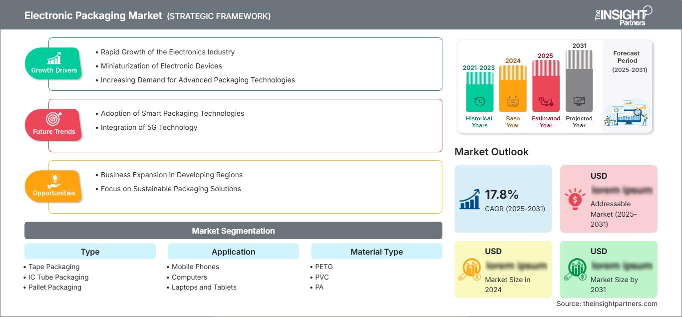
Electronic Packaging Market: Strategic Insights
Regional Insights
North America Electronic Packaging Market
North America accounted for 25-27% of the 2025 Electronic Packaging Market share and is anticipated to grow at a 5.2-5.8% CAGR from 2026 to 2034. Incentives for semiconductor fabrication, hardware for data centers, medical electronics, aerospace components, and the electric vehicle supply chain will contribute to demand. Buyers will value ESD protection, traceability, interface capabilities with automation, and fast turnaround for trays, tubes, tapes, pallets, and packaging.
The Electronic Packaging Market in the United States drives consumption, but Canada will provide medical technology and manufacturing capabilities and Mexico will drive electronics and automotive manufacturing. Sourcing locally means that tooling, thermoforming, extrusion, and technical support services are preferred over feed stock even though it may be sourced globally. Limitations include resin costs, clean manufacturing facilities, and time-consuming validations. Providers who can offer simulation, prototyping, on-line trials, failure analysis, and two sites for production will mitigate risk of program failure.
U.S. Electronic Packaging Market
The US Electronic Packaging Market constituted 80-84% of the revenues in North America in 2025 and is anticipated to grow at a CAGR of 5.3-5.9% through 2034. New chip factories, advanced packaging facilities, AI servers, military electronics, electric vehicles, sensors, and local manufacture of medical devices increase demand. Applications in integrated circuits and printed boards focus on cleanliness, dimensional stability, controllable surface resistivity, proper orientation, clean ejection, and reliable high-speed feed.
AMETEK, Inc., Dordan Manufacturing, Inc., DuPont de Nemours, Inc., Sealed Air Corporation, Sonoco Products Company, and UFP Technologies, Inc. have relevant manufacturing, engineering, or customer service operations in the US. Applications are moving towards higher tolerance trays, moisture protection of sensitive components, reusability, and manufacturing execution system-integrated packaging. Purchasers are demanding long-term quality performance history, regulatory compliance documentation, and alternative source arrangements before agreeing to use particular forms for safety or continuous automated assembly.
Europe Electronic Packaging Market
The Europe Electronic Packaging Market represented 20-22% of revenue in 2025 and is expected to register CAGRs of 4.8-5.4% through 2034. Germany is leading due to its strengths in automotive electronics, industrial controls, sensors, medical devices, and semiconductor manufacturing. Packaging and waste management regulations drive recyclability, reusability, and right sizing needs while presenting opportunities for fibers and high-performance thermoformables with recovery solutions.
The UK promotes compound semiconductor materials, aerospace and defense, and medical technology; thus, maintaining specialty packaging volumes. Germany enjoys economies of scale in automotive and industrial electronics. France utilizes aerospace, defense, and healthcare manufacturing; Italy provides machinery and appliance electronics; and Spain adds automotive, renewable energy, and contract manufacturing applications. Europe’s procurement focuses on declarations, lifecycle data, chemical regulation, and technical support in the region, making it beneficial for packaging suppliers who can redesign their packages without impacting ESD protection, cleanliness, cushioning, and automation.
APAC Electronic Packaging Market
Asia Pacific held 43–45% in 2025 and should achieve a 6.3–6.9% CAGR through 2034. China leads through electronics assembly, displays, batteries, and components; Japan supplies precision materials and automation; South Korea concentrates memory, sensors, and consumer devices.
India is adding mobile-device and semiconductor capacity through localization programs, while Australia contributes medical and industrial electronics demand. Integrated supply chains, manufacturing scale, skilled conversion, and policy-backed investment reinforce regional leadership, although price pressure and export controls increase the value of reusable systems and localized technical service.
Middle East & Africa Electronic Packaging Market
The Middle East & Africa market is projected to expand at a 4.5–5.1% CAGR through 2034. Saudi Arabia leads through industrial diversification, localized electronics, data centers, and energy infrastructure, while the UAE supports logistics, technology investment, and regional distribution.
South Africa contributes automotive, medical, mining, and industrial electronics demand. Rest-of-MEA opportunities center on imported components and finished devices supported by local protective-packing conversion. Limited specialized tooling and ESD-validation infrastructure favor distributor partnerships, technical-service hubs, and phased capacity near assembly and logistics clusters.
Segmentation Analysis
Type
The Type segment is projected to grow at a 5.6–6.2% CAGR during 2026–2034. Electronic Packaging Market scope spans automated component feeding, intermediate handling, storage, and outbound transport. Selection depends on component geometry, electrostatic sensitivity, line speed, cleanliness, stackability, reuse cycles, and logistics intensity. Tray Packaging remains the largest format because it protects and orients varied components, while Tape Packaging gains from high-throughput surface-mount assembly.
- Tape Packaging: Carrier and cover tapes enable indexed, high-speed component presentation, supporting surface-mount automation where pocket accuracy, peel force, antistatic performance, and reel integrity influence yield.
- IC Tube Packaging: Extruded tubes provide economical linear storage and feeding for standardized packages, remaining strategically important for controlled orientation, stackability, identification, and repeated handling between process steps.
- Pallet Packaging: Pallets consolidate larger devices, modules, and reusable dunnage for plant-to-plant movement, emphasizing load stability, cushioning, forklift efficiency, traceability, and reverse-logistics economics across industrial supply chains.
- Tray Packaging: Matrix trays lead through versatile pocket designs, reliable stacking, automated loading, and robust protection for ICs, sensors, and precision assemblies during testing, storage, and shipment.
Application
The Application segment is forecast to advance at a 6.0–6.6% CAGR during 2026–2034. Mobile phones, computers, medical instruments, sensors, and ICs require different combinations of ESD protection, cushioning, cleanliness, and automated presentation. ICs offer the highest growth because advanced logic, memory, power devices, and heterogeneous packages carry greater value and tighter tolerance requirements. Finished-device packaging increasingly balances protection, sustainability, and unboxing efficiency.
- Mobile Phones: High-volume launches require compact, lightweight, presentation-ready packs and component carriers that protect displays, cameras, processors, and connectors while supporting rapid global fulfillment and recycling targets.
- Computers: Broad configurations create demand for protective inserts, accessory organization, and reusable component handling, with procurement balancing shock resistance, pack density, branding, and automated kitting efficiency.
- Laptops and Tablets: Thin, high-value devices need precise cushioning, screen protection, compact accessories, and damage-resistant transit structures, making right-sizing and fiber substitution important design priorities.
- Desktops and Servers: Heavier systems and dense electronics require robust corrugated structures, foam or molded protection, moisture control, and component-level packaging suited to data-center installation and replacement logistics.
- Medical Instruments: Sensitive instruments demand clean, traceable, tamper-aware packaging with dependable cushioning and documentation, particularly where optical, diagnostic, monitoring, or portable devices face regulated distribution environments.
- Sensors: Miniaturized sensors require accurate orientation, ESD protection, particulate control, and automated feeding, creating strategic demand for tight-tolerance tapes, tubes, and trays across automotive and industrial programs.
- ICs: Logic, memory, analog, and power devices need standardized, ESD-safe presentation formats that protect leads and surfaces while enabling inspection, testing, storage, and high-speed assembly.
Material Type
The Material Type segment is expected to register a 5.7–6.3% CAGR during 2026–2034. PETG, PVC, PA, and PS offer different balances of transparency, stiffness, thermoformability, moisture behavior, chemical resistance, and cost. Material choice also reflects ESD additives, recycled-content goals, cleanroom suitability, and recovery infrastructure. PETG gains where clarity and forming are important, while PA serves demanding durability and barrier requirements despite higher cost.
- PETG: Clear, tough, and readily thermoformed PETG supports trays, clamshells, and device packs where visibility, impact resistance, dimensional detail, and potential recycled-content integration matter.
- PVC: PVC offers established forming performance, clarity, stiffness, and cost control, but regulatory scrutiny and customer material restrictions increasingly require documented recovery routes or alternative specifications.
- PA: Polyamide delivers strength, abrasion resistance, and useful barrier performance for demanding handling environments, supporting specialized tubes, films, and protective components where durability outweighs resin cost.
- PS: Polystyrene remains economical and easy to thermoform for rigid trays and inserts, serving high-volume programs that prioritize pocket precision, stackability, light weight, and process familiarity.
Opportunity Snapshot
| Application | Revenue Contribution | Trend Tag | Adoption Stage |
| Mobile Phones | High | Compact Packs | Mature |
| Computers | Medium | Fiber Migration | Mature |
| Laptops and Tablets | High | Right Sizing | Mature |
| Desktops and Servers | High | AI Servers | Scaling |
| Medical Instruments | Medium | Clean Protection | Scaling |
| Sensors | Medium | Precision Feeding | Scaling |
| ICs | High | ESD Control | Scaling |
| Others | Low | Custom Handling | Emerging |
Electronic Packaging Market Growth Drivers and Impact Analysis
Semiconductor Capacity Raises Qualified Packaging Demand
Billings for semiconductor equipment came to US$ 135.1 billion in 2025, an increase of 15%, while those of assembly and packaging equipment increased by 21%. This investment increases the number of handling processes of wafers, dies, final ICs, and modules, thus boosting the need for carrier tapes, tubes, JEDEC trays, clean containers, and reusable handling equipment. The market effect is limited to smaller pocket geometry, reduced contamination, electrostatic control, and change management. Packaging companies that are involved in the process qualification phase will be able to stay specified in several production cycles. It becomes more difficult for new entrants since their customers demand statistical capability, lot traceability, materials declarations, and multi-site supply capability.
Device Miniaturization Increases Protection Complexity
The smaller parts, narrower lead spacing, exposed optics, and increased packing make static discharge, particulate contamination, vibrations, and orientation errors more intolerable. With increasing functions packed into portable electronic devices, sensors, wearable technologies, servers, and healthcare equipment, the packaging needs to accommodate more value in smaller spaces without sacrificing speed in automated placement. The business case extends beyond the size of individual units since the tighter tolerances make more tooling, inspection, and testing activities necessary per package. This value is achievable through the combination of digital cavity design, simulations, prototypes, conductive materials, and line trials. The standardization of package exteriors with custom interiors makes this possible.
Automation and Logistics Favor Consistent Pack Geometry
The speed of assembling, automated handling of materials, automated storage facilities, and global contract manufacturing make it so that packaging geometry is a factor in production efficiency. A warping tray, inaccuracies of the tube, cover tape seal defects, and unstable pallets can interfere with machines, break down components, and lead to tracing problems that are costly to solve. Therefore, customers evaluate the packaging not just according to its material price but also taking into account such factors as feeding capacity, stacking, scanning, cycle time, and overall handling costs. The purchasing approach becomes that of favoring those manufacturers who provide process capability data, tooling control, preventive maintenance, and technical support.
Electronic Packaging Market Future Trends
Smart, Traceable Packaging Enters Production Loops
Electronic Packaging market trends will see a convergence between trays, reels, tubes, and pallets with labels that have serialization, RFID tags, environmental sensors, and manufacturing information. It is not consumer-oriented, rather it is production-oriented. The aim is to be able to identify the product, track its location, reuse rate, moisture exposure, and whether it is ready on-line side or not. The implementation will start with expensive ICs, medical equipment, aerospace electronics, and reusable logistics carriers because a missing or corrupted package will be highly costly. The vendors that provide durability, readability, secure data transfer, and cleanable identification can help in achieving better inventory control and incident investigation.
Circular Materials and Reusable Format Platforms
Due to regulatory influences and consumer objectives of waste reduction, packaging will rely on recycled sheet, fiber alternatives, downgauging, monomaterial designs, and reusable formats. Performance should never suffer, so research and development activities will focus on making sure that there is sufficient surface protection, pocket location, impact performance, cleanliness, and dimensions in successive runs. Digital passports and materials declarations will enable better recovery options, while standardized footprints will allow shared machinery to make sense for production facilities. The winners will be focused on cost per protected unit rather than selling sustainability as an idea. Collaboration with resin suppliers, recyclers, cleaners, logistic providers, and machinery providers will be needed, since circularity means recovery infrastructure and not material selection.
Electronic Packaging Market Opportunities
Regional Clean Packaging and Rapid-Tooling Centers
The clean thermoforming, extrusion, slitting, tooling, and validation centers can be set up around semiconductor, sensor, medical device, and electronics hubs in North America, India, South East Asia, and Eastern Europe. The business model needs to involve small batch development, scalable recipe, ESD testing, dimensional measurement, and technical field service. Revenue opportunities could include design, prototype, tooling, qualification, conversion, cleaning, and ultimately production supplies. Collaboration with machine suppliers and institutes can help address any capability gaps. The process transfer through two locations will assure the consistency for multinationals. The success will depend on qualified pipelines and anchor projects, not on speculative commodity facilities or single cycle of applications.
Reusable Packaging-as-a-Service for Component Flows
The ability for reusable trays, pallets, and dunnage to become an investment is enabled when a single supplier manages the design, ownership, tracking, cleaning, maintenance, and return logistics processes of the packaging. This is enabled by Electronic Packaging Market Forecasts in closed-loop systems in semiconductors, automobiles, servers, and medical device industries where packaging moves back-and-forth between known locations. Contracts must be structured to base fees on availability, loss, cycle time, and contamination effectiveness rather than units sold. Dimensionally consistent outer shell with exchangeable inserts will enable changes in product without losing automation capability. The early program must focus on lanes with guaranteed returns and then grow through digital asset management and common cleaning facilities.
Recent Developments
- October 2025: Rapidus is exploring an ambitious advanced packaging strategy that uses large glass substrates and panel-level packaging (PLP) to support next-generation AI and high-performance processors. Instead of relying on conventional 300 mm silicon wafers, the Japanese chipmaker is developing 600 mm × 600 mm glass panels, which can accommodate significantly more chiplets and interposers in a single manufacturing run. This approach has the potential to reduce production costs, improve manufacturing efficiency, and enable larger, more complex chip designs for AI and HPC applications.
- July 2025: Cosmo Plastech, the rigid packaging business of Cosmo Films, a global leader in specialty films, announces the launch of its Electrostatic Discharge (ESD) Plastic Sheet (PET) – a specially engineered solution developed to support the critical needs of India’s rapidly expanding electronics and device manufacturing ecosystem.
- June 2026: Qnity Electronics, Inc. (“Qnity”) (NYSE: Q), a premier technology solutions leader across the semiconductor value chain, announced the launch of its Advanced Packaging Innovation Hub, underscoring advanced packaging as a strategic growth driver and innovation priority for the company. The new online platform showcases Qnity’s breadth of material and technology solutions designed for advanced packaging, enabling the next generation of artificial intelligence (AI), high-performance computing, cloud, networking, and edge computing systems.
Frequently Asked Questions

- Comprehensive Market Sizing and Forecast Analysis
- Detailed Segmentation Analysis
- In-Depth Market Dynamics Assessment
- Regional and Country-Level Insights
- Competitive Landscape and Company Benchmarking
- Strategic Business Intelligence
Recent Reports
Testimonials

The Insight Partners provided valuable market intelligence that supported our global go-to-market strategy. Their team was professional, responsive, and attentive to our feedback, providing thoughtful analysis and helpful methodological clarifications throughout the project.
Junmo Kim Chief Financial Officer (CFO), Enertech Co., Ltd.
The Insight Partners' SCADA System Market report is comprehensive, with valuable insights on current trends and future forecasts. The team was highly professional, responsive, and supportive throughout. We are very satisfied and highly recommend their services.
RAN KEDEM Partner, Reali Technologies LTDs
I requested a report on a very specific software market and the team produced the report in a few days. The information was very relevant and well presented. I then requested some changes and additions to the report. The team was again very responsive and I got the final report in less than a week.
JEAN-HERVE JENN Chairman, Future Analytica
We worked with The Insight Partners for an important market study and forecast. They gave us clear insights into opportunities and risks, which helped shape our plans. Their research was easy to use and based on solid data. It helped us make smart, confident decisions. We highly recommend them.
PIYUSH NAGPAL Sr. Vice President, High Beam Global
The Insight Partners delivered insightful, well-structured market research with strong domain expertise. Their team was professional and responsive throughout. The user-friendly website made accessing industry reports seamless. We highly recommend them for reliable, high-quality research services
YUKIHIKO ADACHI CEO, Deep Blue, LLC.
This is the first time I have purchased a market report from The Insight Partners.While I was unsure at first, I visited their web site and felt more comfortable to take the risk and purchase a market report.I am completely satisfied with the quality of the report and customer service. I had several questions and comments with the initial report, but after a couple of dialogs over email with their analyst I believe I have a report that I can use as input to our strategic planning process.Thank you so much for taking the extra time and making this a positive experience.I will definitely recommend your service to others and you will be my first call when we need further market data.
JOHN SUZUKI President and Chief Executive Officer, Board Director, BK Technologies
I wish to appreciate your support and the professionalism you displayed in the course of attending to my request for information regarding to infectious disease IVD market in Nigeria. I appreciate your patience, your guidance, and the fact that you were willing to offer a discount, which eventually made it possible for us to close a deal. I look forward to engaging The Insight Partners in the future, all thanks to the impression you have created in me as a result of this first encounter.
DR CHIJIOKE ONYIA MANAGING DIRECTOR, PineCrest Healthcare Ltd.Reason to Buy
- Informed Decision-Making
- Understanding Market Dynamics
- Competitive Analysis
- Identifying Emerging Markets
- Customer Insights
- Market Forecasts
- Risk Mitigation
- Boosting Operational Efficiency
- Strategic Planning
- Investment Justification
- Tracking Industry Innovations
- Aligning with Regulatory Trends





 Get Free Sample for