
SiC on Insulator Substrate Market Demand, Trends & Forecast by 2034
SiC on Insulator Substrate Market Size and Forecasts (2021–2034), Global and Regional Share, Trends, and Growth Opportunity Analysis Report Coverage : By Application (Power Electronics, RF Devices, LEDs, Solar Cells), Material Type (Silicon Carbide, Gallium Nitride, Silicon), Wafer Size (Small Wafer, Medium Wafer, Large Wafer), End Use Industry (Consumer Electronics, Automotive, Telecommunications, Renewable Energy)
- Status : Data Released
- Report Code : TIPRE00039625
- Category : Electronics and Semiconductor
- No. of Pages : 150
- Available Report Formats :


- Last update date : July 17, 2026


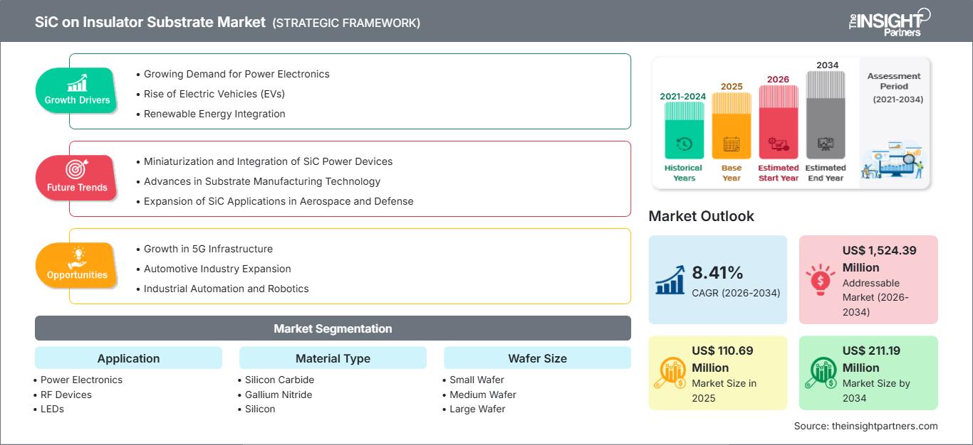
2025 Market Size
US$ 110.69 Mn
Base year value
2034 Forecast
US$ 211.19 Mn
Projected by 2034
CAGR 2026-2034
8.41 %
Growth rate
Addressable Market
US$ 1,524.39 Mn
(2026-2034)
The SiC on Insulator Substrate Market was valued at US$ 110.69 Million in 2025 and is projected to reach US$ 211.19 Million by 2034; it is expected to register a CAGR of 8.41% during 2026–2034. The outlook reflects rising use of engineered substrates in power electronics, RF devices, LEDs, and solar cells, where thermal stability, electrical isolation, and compact device architecture remain central purchasing criteria.
Across North America, the SiC on Insulator Substrate Market size is supported by a modeled CAGR range of 7.9–8.6% through 2034, reflecting demand from EV power conversion, 5G RF front ends, and defense-grade high-frequency systems. Regional traction is reinforced by U.S. wafer capability, reshoring incentives, and wider adoption of 150 mm and 200 mm compound semiconductor platforms.
SiC on Insulator Substrate Market Assessment and Insights
- North America represented 31–34% share in 2025 and is expected to grow at a CAGR of 7.9–8.6% during 2026–2034, supported by EV electronics, RF infrastructure, and domestic substrate capacity.
- US accounted for 72–76% of North America in 2025 and is projected to grow at a CAGR of 8.0–8.7%, helped by SiC device investment and telecom demand.
- Europe held 24–27% share in 2025 and is expected to expand at a CAGR of 7.4–8.1%, led by Germany, France, Italy, the UK, and Spain.
- Asia Pacific captured 30–33% share in 2025 and is projected to grow at a CAGR of 9.0–9.8%, led by China, Japan, South Korea, and India.
- Largest Segment Power Electronics held 39–43% market share in 2025 and is expected to grow at a CAGR of 8.5–9.2% during 2026–2034.
- High Growth Segment RF Devices held 24–28% market share in 2025 and is expected to grow at a CAGR of 9.4–10.2% during 2026–2034.
- Key companies analyzed in detail: Infinera Corporation, STMicroelectronics N.V., Skyworks Solutions, Inc., onsemi, Geneva Silicon LLC, Mouser Electronics, Inc., Nexperia B.V., Infineon Technologies AG, Wolfspeed, Inc., NXP Semiconductors N.V.
Source: The Insight Partners' analysis based on proprietary research, government publications, company annual reports, investor presentations, industry databases, and expert interviews.
Market progress has shifted from lab-sized bonded wafers to application-specific engineered substrates that minimize parasitic capacitances and enhance heat dispersion. There is a shift in production characteristics, as suppliers now focus on qualifying bigger wafer sizes, improving epitaxial control and lowering defect densities. Increasingly, the SiC on Insulator Substrate Market relies on integration between substrate experts, end-device manufacturers and module makers, as yield, bonding uniformity, and wafer supplies influence commercial implementation in automotive, telecommunications and renewable energy applications.
Future demands will not only increase within existing automotive and RF customers, but will also expand as new energy efficiency regulations, grid modernization projects and semiconductor incentives in certain regions drive broader qualifications. Developing activities in Asia Pacific and selected European clusters may bring supply diversification, while North America companies continue to prefer safe sources. This market will favor suppliers capable of delivering scalable wafers, material consistency, and application expertise in power dense devices operating at high voltage and high frequency.
SiC on Insulator Substrate Market Report Scope
| Report Attribute | Details |
|---|---|
| Market size in 2025 | US$ 110.69 Million |
| Market Size by 2034 | US$ 211.19 Million |
| Global CAGR (2026 - 2034) | 8.41% |
| Historical Data | 2021-2024 |
| Forecast period | 2026-2034 |
SiC on Insulator Substrate Market Analysis
The factors affecting the demand have been the emergence of EV inverters, fast charger systems, solar invertor, and radio frequency systems that require reduced switching losses and heat dissipation capabilities. The increase in the SiC On Insulator Substrate Market is due to the transition from conventional silicon substrate to engineered substrates for smaller layouts and enhanced voltage withstand ability.
The supply chain includes crystal growth, wafer slicing, bonding, polishing, epitaxy, device processing, assembly, and shipment. The supply chain is limited due to the relatively slow crystal growth rate of SiC compared to silicon and challenges in achieving defect free crystals. Larger wafers reduce cost per die provided bonding yield, surface finish, and thermal interface do not vary between lots.
Competitive positioning is being increasingly harmonized. STMicroelectronics N.V., onsemi, Infineon Technologies AG, Wolfspeed, Inc., and NXP Semiconductors N.V. are matching up their product offerings with wafer manufacturing strategies, either internally or through partnerships, with Skyworks Solutions, Inc. and Infinera Corporation adding their value in terms of demand insights via RF and optical communications respectively. Mouser Electronics, Inc. offers its availability in prototyping and engineering segments.
In SiC on Insulator Substrate Market analysis, it is observed that suppliers offering 200 mm wafer roadmaps, automotive qualification capability and RF design capabilities would fare better from a pricing perspective. Geneva Silicon LLC and Nexperia B.V. reflect the importance of specialty materials and discrete devices, while big semiconductor corporations rely on long term contracts, regional manufacturing capabilities and applications specific modules.
● REPORT CUSTOMIZATION
Tailor This Report To Align With Your Specific Business Requirements
This report can be customized to align precisely with your business objectives, scope, and target markets. Customization options include tailored segmentation, geography, competitive analysis, and strategic insights to support informed decision-making.
Customize This Report →WHAT YOU CAN ADJUST
- ● Segmentations
- ● Geography
- ● Competitive Analysis
- ● Language Preferences
SiC on Insulator Substrate Market: Strategic Insights
Regional Insights
North America SiC on Insulator Substrate Market
North America accounted for 31–34% of global revenue in 2025 and is modeled to expand at a CAGR of 7.9–8.6% during 2026–2034. The SiC on Insulator Substrate Market share in the region is supported by EV inverter development, aerospace electronics, advanced RF systems, and federal incentives that encourage domestic semiconductor capability.
In addition to that, the market is further aided by concentration in design engineering, reliability packaging, and early adoption of wide-bandgap technology in the charging infrastructure. The customers are opting for dual sourcing following the recent supply disruptions, which favors the assessment of engineered substrates. Growth of North America is forecasted to continue in a disciplined manner due to long qualification cycles.
U.S. SiC on Insulator Substrate Market
United States accounted for 72–76% of North American demand in 2025 and is anticipated to exhibit a CAGR of 8.0–8.7% between 2026 and 2034. The traction factors driving the market include power electronics initiatives, radio frequency defense, artificial intelligence (AI) data center power supply systems, and industrial electrification due to high thermal conductivity and switching efficiency that merit qualification expenses.
Market players in this region include companies like Wolfspeed, Inc., Skyworks Solutions, Inc., onsemi, Infinera Corporation, and Mouser Electronics, Inc. driving various market layers in the value chain. The regions with strong application momentum in the US are traction inverters, RF front-end, satellite communications, and power conversion. Buyers in the US will prefer vendors with wafer roadmap stability.
Europe SiC on Insulator Substrate Market
Europe has a share of 24-27% in 2025 and will witness growth at CAGR of 7.4–8.1% till 2034, and Germany is leading among all countries. The United Kingdom will contribute towards compound semiconductors and RF design, whereas Germany will contribute due to its expertise in automotive power electronics and industrial drives that require substrates qualified for high voltage switching and lifetime operation.
France has the contribution of its efforts in the research of power devices, photonics, and semiconductor resilience from the government. Italy will be significant due to the manufacturing investments of SiC and automotive devices. Spain will also have its contributions due to renewable energy installations and grid upgrades.
APAC SiC on Insulator Substrate Market
In 2025, APAC had a market share of 30-33% and is estimated to experience the highest CAGR of 9.0-9.8% between 2026 and 2034. China emerges as the top country market because of EV penetration, local wafer manufacturing, and localization of power modules. Japan and South Korea focus on high-quality materials and device reliability.
India and Australia get momentum from renewable energy technology, charging infrastructure, and industrial electrification. The various governmental initiatives that have been taken by countries related to semiconductors independence, green energy technology, and telecom infrastructure upgrades increase the demand visibility. Yield consistency in advanced substrate technology is the greatest constraint of the region.
Middle East & Africa SiC on Insulator Substrate Market
Middle East & Africa is expected to grow at a CAGR of 6.8–7.5% during 2026–2034, with the UAE leading near-term adoption. Saudi Arabia and the UAE are investing in renewable power, smart infrastructure, and industrial diversification, which creates opportunities for high-efficiency converters and grid-connected electronics.
The South African component would include mining, telecoms, and solar projects as well as mine electrification, whereas the Rest of MEA will still be project-based. It is expected that adoption will proceed through importation of power modules as opposed to wafers manufacturing locally. There is a lot of interest in substrates for improved thermal behavior.
Segmentation Analysis
Application
Application is expected to grow at a CAGR of 8.6–9.3% during 2026–2034, supported by device-level efficiency requirements across conversion, communication, illumination, and renewable generation. SiC on Insulator Substrate Market scope in this segment is defined by the ability to deliver isolation, thermal control, and lower capacitance in compact architectures without compromising reliability or manufacturability.
- Power Electronics remains the largest application because EV inverters, fast chargers, industrial drives, and solar converters require high-voltage operation, reduced switching loss, and durable thermal performance.
- RF Devices show strong demand from 5G, satellite, radar, and microwave systems, where substrate isolation and heat handling improve signal integrity at elevated frequencies.
- LEDs use advanced substrates where thermal spreading and lattice compatibility help improve device reliability, especially in high-brightness lighting and specialty display applications.
- Solar Cells benefit from efficient conversion electronics and durable materials that support inverter miniaturization, distributed generation, and long service life in outdoor operating environments.
Material Type
Material Type is projected to grow at a CAGR of 8.1–8.8% during 2026–2034. Material selection is driven by the trade-off between cost, thermal conductivity, breakdown strength, and integration complexity. Silicon carbide leads high-power use cases, gallium nitride is advancing in high-frequency and compact power designs, and silicon remains relevant where mature manufacturing and cost control outweigh performance extremes.
- Silicon Carbide is strategically important for high-voltage and high-temperature environments, with strong fit in EV traction, grid conversion, industrial drives, and aerospace power systems.
- Gallium Nitride addresses fast-switching and RF-centric designs, especially where compact power density, high frequency, and lower system weight create measurable performance advantages.
- Silicon remains valuable in cost-sensitive platforms and hybrid integration, providing a familiar manufacturing base for applications that do not require extreme wide-bandgap performance.
Wafer Size
Wafer Size is expected to expand at a CAGR of 8.4–9.0% during 2026–2034 as producers migrate toward larger diameters to improve die output and process economics. The shift is not purely scale-driven; it requires tighter control of bow, bonding, polishing, and defect density. Customers evaluate wafer size alongside yield maturity and device qualification risk.
- Small Wafer supports research, prototyping, and specialty production where flexibility, lower batch volume, and rapid process iteration are more important than die cost optimization.
- Medium Wafer balances availability and manufacturing learning curves, making it practical for early commercial programs, RF devices, and controlled expansion of power applications.
- Large Wafer is strategically important for cost reduction and volume scalability, especially as 200 mm platforms become more relevant for automotive and industrial power electronics.
End Use Industry
End Use Industry is projected to grow at a CAGR of 8.3–9.1% during 2026–2034. Demand differs by qualification cycle: automotive requires long validation, telecommunications values RF efficiency and reliability, renewable energy prioritizes conversion losses, and consumer electronics favors compact power management. Supplier success depends on matching substrate performance with application-specific cost and durability thresholds.
- Consumer Electronics offers selective opportunities in compact chargers, high-efficiency adapters, and advanced displays, but adoption depends on cost reduction and proven manufacturing repeatability.
- Automotive is a core demand base because EV traction systems, onboard chargers, and battery management architectures value high efficiency, temperature tolerance, and compact modules.
- Telecommunications supports RF-oriented demand through base stations, satellite links, microwave equipment, and optical networking systems requiring stable high-frequency performance.
- Renewable Energy benefits from solar inverters, storage converters, and grid-edge electronics where lower losses improve lifetime energy yield and system reliability.
Opportunity Snapshot
| Application | Revenue Contribution | Trend Tag | Adoption Stage |
| Power Electronics | High | Fast Charging | Scaling |
| RF Devices | Medium | 5G Radios | Scaling |
| LEDs | Low | Thermal LEDs | Emerging |
| Solar Cells | Medium | Solar Inverters | Scaling |
SiC on Insulator Substrate Market Growth Drivers and Impact Analysis
Electrified Mobility Requires Higher Conversion Efficiency
The proliferation of electric vehicles leads to increased demand for substrates which can help achieve reduced losses of inverters, onboard charger, and DC-DC converter architectures. The increased use of 800 volts architecture makes it valuable to have materials that can function at high voltages and help in achieving heat dissipation. Silicon Carbide based platforms can help reduce stress in devices, improve switch performance, and provide for small coolers. This will be most effective in situations where manufacturers are trying to extend the driving range of electric vehicles through capacity expansion without having to change the battery size.
RF Infrastructure Needs Stable High-Frequency Materials
Telecommunications networks are moving toward denser radio deployments, higher frequency bands, and more power-efficient front ends. RF devices built on insulated SiC-based platforms can offer improved isolation, thermal stability, and lower parasitic effects, which are important in base stations, satellite communications, radar, and microwave systems. The effect on demand is not limited to volume; it also raises specification requirements for surface quality and uniformity. Suppliers that can support RF engineers with consistent wafers, low-loss interfaces, and predictable thermal behavior are positioned to win design-ins where qualification cycles are technically rigorous.
Renewable Power Conversion Raises Reliability Standards
Solar, storage, and grid-edge systems require converters that operate efficiently over long service lives in variable environmental conditions. Substrate performance matters because thermal cycling, humidity exposure, and sustained high-voltage switching can accelerate failure in power devices. Advanced insulated substrates can help reduce losses, shrink inverter footprints, and improve durability in distributed energy systems. The commercial impact is visible in lower maintenance needs and improved lifetime energy output. Utilities and renewable developers are expected to adopt the technology through qualified power modules rather than direct wafer procurement, making device partnerships essential.
SiC on Insulator Substrate Market Future Trends
Migration Toward 200 mm Engineered Wafer Platforms
One of the defining SiC on Insulator Substrate Market trends is the gradual transition toward larger engineered wafers that can improve die economics and support higher-volume device manufacturing. The trend will depend on bonding yield, crystal defect management, and compatibility with existing fab equipment. As 200 mm capability improves, substrate suppliers may offer more standardized specifications, reducing customer qualification time. This shift should also encourage greater participation by foundries, packaging houses, and module suppliers that require predictable wafer formats for automated production and cost modeling.
Hybrid Material Integration for Power and RF Systems
Future architectures are likely to combine SiC, GaN, and silicon-based layers to balance cost, voltage capability, frequency response, and thermal performance. Hybrid integration can help designers target application-specific performance rather than relying on one material platform for all requirements. This trend may be especially relevant for compact chargers, RF modules, optical communication components, and renewable energy converters. Suppliers with bonding, epitaxy, and interface engineering expertise will gain strategic advantage as customers seek substrates that support multi-function devices and reduce system-level complexity.
SiC on Insulator Substrate Market Opportunities
Application-Specific Substrate Qualification Programs
Manufacturers can create value by building qualification programs tailored to EV traction, RF infrastructure, renewable converters, and industrial power systems. SiC on Insulator Substrate Market Forecasts point to stronger adoption where suppliers reduce customer uncertainty through reliability data, thermal modeling, and joint device validation. The opportunity is not only selling wafers; it is becoming part of the customer’s design roadmap. Companies that provide application notes, failure-mode analysis, and scalable wafer supply can shorten design cycles and improve conversion from sampling to long-term contracts.
Regional Supply Partnerships for Secure Semiconductor Sourcing
Supply security has become a purchasing criterion for automotive, defense, telecom, and energy customers. Vendors can capture opportunity by forming regional partnerships that combine substrate production, device fabrication, and module assembly near end markets. Such models reduce logistics exposure, improve traceability, and align with government incentives for semiconductor resilience. The opportunity is strongest in North America, Europe, and Asia Pacific clusters where customers need long-term assurance on wafer availability. Partnerships may also support shared yield learning, improving cost competitiveness without sacrificing quality requirements.
Recent Developments
- June 2026: Wolfspeed, an industry leader in silicon carbide, has introduced its fifth technology generation, demonstrating a substantial performance leap in efficiency for next-generation 1200 V and 750 V automotive and industrial applications.
- May 2026: USI, a global leader in electronic design and manufacturing services, today announced a breakthrough in advanced power semiconductor packaging technology designed for next-generation power solutions. Leveraging its innovative substrate and module integration capabilities, USI has successfully embedded silicon carbide (SiC) dies into multilayer ABF substrates and adopted Single-Side Copper Exposed (SSC) module packaging technology to integrate ceramic substrate insulation and wire-bondless architecture within industry-standard power packages.
- August 2024: As global decarbonization efforts drive demand for power semiconductors, Infineon Technologies AG has officially opened the first phase of a new fab in Malaysia that will become the world’s largest and most competitive 200-millimeter silicon carbide (SiC) power semiconductor fab. Malaysian Prime Minister YAB Dato’ Seri Anwar Ibrahim and Chief Minister of the state of Kedah YAB Dato’ Seri Haji Muhammad Sanusi Haji Mohd Nor joined Infineon CEO Jochen Hanebeck, to symbolically launch production.
Frequently Asked Questions

- Comprehensive Market Sizing and Forecast Analysis
- Detailed Segmentation Analysis
- In-Depth Market Dynamics Assessment
- Regional and Country-Level Insights
- Competitive Landscape and Company Benchmarking
- Strategic Business Intelligence
Recent Reports
Testimonials

The Insight Partners' SCADA System Market report is comprehensive, with valuable insights on current trends and future forecasts. The team was highly professional, responsive, and supportive throughout. We are very satisfied and highly recommend their services.
RAN KEDEM Partner, Reali Technologies LTDs
I requested a report on a very specific software market and the team produced the report in a few days. The information was very relevant and well presented. I then requested some changes and additions to the report. The team was again very responsive and I got the final report in less than a week.
JEAN-HERVE JENN Chairman, Future Analytica
We worked with The Insight Partners for an important market study and forecast. They gave us clear insights into opportunities and risks, which helped shape our plans. Their research was easy to use and based on solid data. It helped us make smart, confident decisions. We highly recommend them.
PIYUSH NAGPAL Sr. Vice President, High Beam Global
The Insight Partners delivered insightful, well-structured market research with strong domain expertise. Their team was professional and responsive throughout. The user-friendly website made accessing industry reports seamless. We highly recommend them for reliable, high-quality research services
YUKIHIKO ADACHI CEO, Deep Blue, LLC.
This is the first time I have purchased a market report from The Insight Partners.While I was unsure at first, I visited their web site and felt more comfortable to take the risk and purchase a market report.I am completely satisfied with the quality of the report and customer service. I had several questions and comments with the initial report, but after a couple of dialogs over email with their analyst I believe I have a report that I can use as input to our strategic planning process.Thank you so much for taking the extra time and making this a positive experience.I will definitely recommend your service to others and you will be my first call when we need further market data.
JOHN SUZUKI President and Chief Executive Officer, Board Director, BK Technologies
I wish to appreciate your support and the professionalism you displayed in the course of attending to my request for information regarding to infectious disease IVD market in Nigeria. I appreciate your patience, your guidance, and the fact that you were willing to offer a discount, which eventually made it possible for us to close a deal. I look forward to engaging The Insight Partners in the future, all thanks to the impression you have created in me as a result of this first encounter.
DR CHIJIOKE ONYIA MANAGING DIRECTOR, PineCrest Healthcare Ltd.Reason to Buy
- Informed Decision-Making
- Understanding Market Dynamics
- Competitive Analysis
- Identifying Emerging Markets
- Customer Insights
- Market Forecasts
- Risk Mitigation
- Boosting Operational Efficiency
- Strategic Planning
- Investment Justification
- Tracking Industry Innovations
- Aligning with Regulatory Trends





 Get Free Sample for