
Wafer Cleaning Equipment Market Trends, Size & Growth by 2034
Coverage: by Equipment Type (Single-Wafer Cryogenic Systems, Single-Wafer Spray Systems, Batch Immersion Cleaning Systems, Batch Spray Cleaning Systems, Scrubbers); Wafer Size (300mm, 200mm, 125mm); Functions (Manual Equipment, Automatic Equipment, Semi-Automatic Equipment); Application (LED, MEMS, Memory, RF Device Others) , and Geography (North America, Europe, Asia Pacific, and South and Central America)
- Status : Data Released
- Report Code : TIPRE00004816
- Category : Electronics and Semiconductor
- No. of Pages : 150
- Available Report Formats :


- Last update date : September 22, 2026


2025 Market Size
US$ 8.51 Bn
Base year value
2034 Forecast
US$ 20.05 Bn
Projected by 2034
CAGR 2026-2034
10.00 %
Growth rate
Addressable Market
US$ 127.12 Bn
(2026-2034)
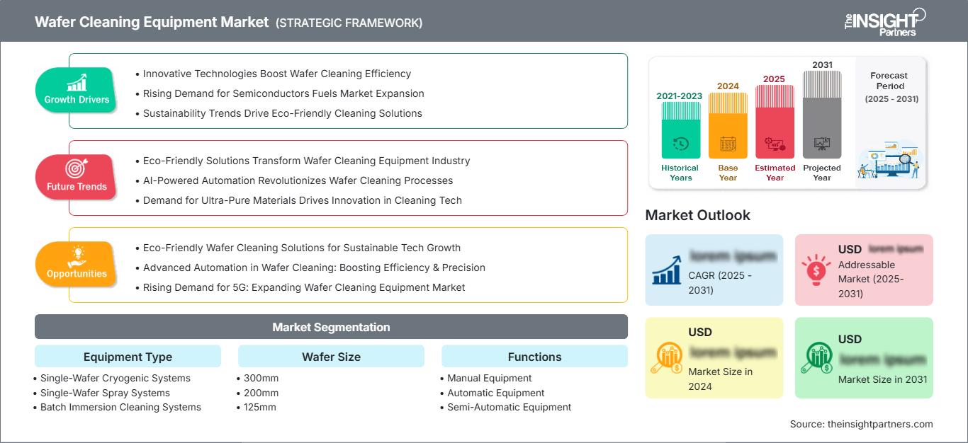
The wafer cleaning equipment market was valued at US$ 8.51 billion in 2025 and is projected to reach US$ 20.05 billion by 2034, growing at a CAGR of 10.00% during 2026–2034. The market reflects rising demand for contamination-control systems used in semiconductor wafer fabrication, advanced packaging, memory, MEMS, RF devices, LEDs, and related microelectronics processes.
North America is expected to maintain a strong position in the wafer cleaning equipment market size outlook, supported by fab localization, advanced logic investments, AI-driven computing demand, and public incentives for semiconductor capacity. Growth in the region is reinforced by 300 mm fab equipment spending, reshoring initiatives, and process-control requirements for high-yield device manufacturing.
Wafer Cleaning Equipment Market Assessment and Insights
- North America: The region is estimated to hold 24–27% share in 2025 and grow at a CAGR of 9.2–10.1% during 2026–2034, driven by advanced-node fabs, AI infrastructure, and domestic manufacturing incentives.
- US: The US accounted for 78–82% of North America in 2025 and is expected to expand at a CAGR of 9.5–10.4% during 2026–2034 as new fabs increase cleaning-tool demand.
- Europe: Europe held 17–20% share in 2025 and is projected to grow at a CAGR of 8.6–9.5% during 2026–2034, led by Germany, France, Italy, the Netherlands, and the UK.
- Asia Pacific: Asia Pacific remained the largest regional base with 42–46% share in 2025 and is forecast to grow at a CAGR of 10.5–11.4% through 2034, supported by China, Japan, South Korea, Taiwan, and India.
- Largest Segment: Single-wafer spray systems held 31–34% share in 2025 and are expected to grow at a CAGR of 9.4–10.3% during 2026–2034, reflecting precision cleaning needs at advanced nodes.
- High Growth Segment: Single-wafer cryogenic systems held 8–11% share in 2025 and are expected to grow at a CAGR of 11.8–12.8% during 2026–2034 as fabs target lower chemical usage and particle removal.
- Key companies analyzed in detail: Applied Materials, Inc.; Entegris, Inc.; FSI International; Modutek Corporation; PVA TePla AG; SCREEN Semiconductor Solutions Co., Ltd.; Semsysco GmbH; SEMES Co., Ltd.; Tokyo Electron Limited; and Veeco Instruments Inc.
Source: The Insight Partners' analysis based on proprietary research, government publications, company annual reports, investor presentations, industry databases, and expert interviews.
The technological evolution in this market has driven the move from general-purpose batch wet processing towards process-oriented platforms, which have better geometry capability, higher wafer productivity and improved defect control. Market growth is expected to come increasingly through EUV lithography, advanced packaging and increased step intensity per wafer. With the rise in complexity of the device structure, fabs are looking for technologies that minimize particle generation, residue, metallic contaminants and chemical residues while not damaging the substrate.
Future demand will be driven by fab construction across regions, AI processors, high bandwidth memory, silicon carbide, gallium nitride, MEMS, and RF devices. Incentives offered by governments in the US, Europe, Japan, South Korea, Taiwan and India are leading to wider geographical spread of wafer fabs. This creates opportunities for equipment suppliers able to support qualification, cleanroom integration, chemical efficiency, and high-volume production requirements, according to the Wafer Cleaning Equipment Market report.
Wafer Cleaning Equipment Market Report Scope
| Report Attribute | Details |
|---|---|
| Market size in 2025 | US$ 8.51 Billion |
| Market Size by 2034 | US$ 20.05 Billion |
| Global CAGR (2026 - 2034) | 10.00% |
| Historical Data | 2021-2024 |
| Forecast period | 2026-2034 |
Wafer Cleaning Equipment Market Analysis
The wafer cleaning equipment market growth is driven by increasingly contamination-sensitive semiconductor processes. More cleaning steps will be required in between deposition, etch, litho, and CMP processes due to the advanced node, which makes surface preparation essential in the overall yield process. The high spend on 300 mm fabrication for AI, high-performance computing, automotive electronics, and memory is expected to drive investments in automatic single-wafer processing systems, batch spray systems, immersion systems, and post-CMP scrubbers.
The chain of value includes tool vendors, chemical companies, ultrapure water system vendors, automation providers, foundries, IDM, OSATs, and compound semiconductor manufacturers. Logic, memory, MEMS, LED, and RF require different cleaning needs, but they are always based on reliable particle removal, low defectivity, and substrate compatibility. The selection of cleaning equipment becomes more dependent on throughput, space saving, chemical savings, and services.
Competitive positioning in the market analysis is determined by process technology, installed base, qualification cycles of customers, and integration with fab automation technologies. SCREEN Semiconductor Solutions Co., Ltd. and Tokyo Electron Limited continue dominating in the advanced cleaning platform segment, while Applied Materials, Inc., Entegris, Inc., SEMES Co., Ltd., Modutek Corporation, PVA TePla AG, Semsysco GmbH, and Veeco Instruments Inc. provide solutions for wet benches, materials handling, thermal processing and specialty substrates.
The investment pattern is switching towards water-saving, chemical-saving, and automated cleaning platforms. Modern fabs have to achieve high performance rates but at the same time comply with environmental standards, take into account expenses for wastewater treatment and restrictions concerning process chemicals usage. Such suppliers that can provide both high performance rates in particle removal and efficient consumable savings will be able to boost their position in the coming years.
● REPORT CUSTOMIZATION
Tailor This Report To Align With Your Specific Business Requirements
This report can be customized to align precisely with your business objectives, scope, and target markets. Customization options include tailored segmentation, geography, competitive analysis, and strategic insights to support informed decision-making.
Customize This Report →WHAT YOU CAN ADJUST
- ● Segmentations
- ● Geography
- ● Competitive Analysis
- ● Language Preferences
Wafer Cleaning Equipment Market: Strategic Insights
Regional Insights
North America wafer cleaning equipment market
North America accounted for an estimated 24–27% wafer cleaning equipment market share in 2025 and is expected to grow at a CAGR of 9.2–10.1% during 2026–2034. Regional Demand is based on US fab investments, logic technology investments, defense electronics, data centers for AI applications, and localization of the supply chain. The region is benefiting from developed R&D eco-systems and high demand for process control equipment.
Cleaning is gaining momentum owing to the qualification of 300 mm capability at advanced fabs and the production of specialty semiconductors. High demand for cleaning equipment is expected in automatic equipment, single wafer spray systems, and post-CMP cleaning.
U.S. wafer cleaning equipment Market
The US represented 78–82% of North America in 2025 and is projected to grow at a CAGR of 9.5–10.4% during 2026–2034. High-throughput cleaning solutions are getting installed because of domestic capacity programs, foundry expansions, and increased demand for AI processors. In addition, the country enjoys good service networks for equipment and semiconductor materials providers.
Application demand in the market is focused on logic, memory, RF devices, MEMS, and power electronics. Large fabs need automatic cleaning solutions that provide process reproducibility, low particles, and a stable chemical supply.
Europe wafer cleaning equipment Market
Europe held 17–20% share in 2025 and is expected to grow at a CAGR of 8.6–9.5% during 2026–2034. Automotive semiconductors, power electronics, and industrial microelectronics drive regional demand from Germany. France, Italy, the Netherlands, Spain, and the United Kingdom generate demand based on research and development, specialty fabs, MEMS, photonics, and innovative ecosystem for equipment.
Quality, traceability, energy efficiency, and eco-conscious production processes are the main characteristics of fabs in Europe. Systems that decrease chemical use and increase particle removal performance attract more interest. Demand growth is the most active where there is a match between semiconductor sovereignty programs and electric vehicles, industrial automation, renewable energy, and defense electronics value chains.
APAC wafer cleaning equipment Market
APAC accounted for 42–46% share in 2025 and is projected to grow at a CAGR of 10.5–11.4% during 2026–2034. China, Japan, South Korea, Taiwan, and India are driving tool demand through foundry, memory, display, compound semiconductor, and electronics manufacturing expansion.
Regional leadership is supported by high wafer-start volumes and strong 300 mm capacity additions. China and South Korea contribute scale, Taiwan supports advanced foundry demand, Japan provides equipment and materials expertise, and India is entering the market through policy-led semiconductor investments.
Middle East & Africa wafer cleaning equipment Market
The Middle East & Africa market is comparatively smaller but is expected to grow at a CAGR of 7.2–8.1% during 2026–2034. The electronics industry is being looked into by Saudi Arabia, the UAE, and South Africa, which are considering selective demand for equipment in the field.
It is expected that opportunities would be available for research facilities, package facilities, specialty electronics, and technology park developments and not the big-scale advanced fabs. Demand will depend on skills, cleanrooms, partnership with suppliers, and the execution of semiconductor policies.
Segmentation Analysis
Equipment Type
Equipment Type is expected to grow at a CAGR of 9.6–10.5% during 2026–2034. The wafer cleaning equipment market scope across equipment types is widening as fabs require the right balance between throughput, precision, cost, and contamination control. Single-wafer platforms serve advanced nodes, while batch and scrubber systems remain relevant in mature and specialty processes.
- Single-Wafer Cryogenic Systems: These systems are gaining strategic relevance where fabs seek strong particle removal and lower chemical usage, especially for advanced substrates, high-value wafers, and environmentally sensitive process modules.
- Single-Wafer Spray Systems: These tools lead demand because they offer precise chemistry control, wafer-level uniformity, and high repeatability for logic, memory, MEMS, and post-etch cleaning applications.
- Batch Immersion Cleaning Systems: Batch immersion tools remain important for cost-effective cleaning in mature nodes, MEMS, LEDs, and specialty wafers where throughput and process simplicity are key priorities.
- Batch Spray Cleaning Systems: Batch spray platforms support medium-to-high throughput operations and are used where fabs need chemical distribution efficiency, wafer handling stability, and repeatable surface conditioning.
- Scrubbers: Scrubbers are essential for post-CMP cleaning and particle removal, especially in processes where mechanical residue, slurry particles, and surface debris can affect downstream yield.
Wafer Size
Wafer Size is projected to grow at a CAGR of 9.8–10.7% during 2026–2034. The transition toward 300 mm capacity remains a major driver, while 200 mm and 125 mm tools continue to support analog, MEMS, LED, RF, and compound semiconductor processes.
- 300mm: The 300 mm segment dominates tool demand because advanced logic, memory, and high-volume fabs require automated cleaning platforms with tight particle control and strong process repeatability.
- 200mm: The 200 mm segment remains resilient in power devices, RF components, MEMS, and automotive electronics, where mature-node capacity continues to operate at high utilization.
- 125mm: The 125 mm segment serves niche and specialty applications, including LEDs, research lines, and selected compound semiconductor production where smaller wafer handling remains practical.
Functions
Functions are expected to grow at a CAGR of 9.3–10.2% during 2026–2034. Automatic equipment is gaining share as fabs pursue higher throughput, lower variability, and stronger process control. Manual and semi-automatic tools remain useful in pilot lines, specialty fabs, and lower-volume production.
- Manual Equipment: Manual tools are used in research, low-volume production, and specialty processes where flexibility, lower capital cost, and operator-controlled processing remain valuable.
- Automatic Equipment: Automatic systems are preferred in high-volume fabs because they reduce handling risk, improve repeatability, support recipe control, and integrate with fab automation platforms.
- Semi-Automatic Equipment: Semi-automatic tools bridge cost and productivity needs, supporting specialty manufacturers that require better consistency without the full capital intensity of automated platforms.
Application
Application is forecast to grow at a CAGR of 9.7–10.6% during 2026–2034. Memory, RF devices, MEMS, and LEDs rely on clean wafer surfaces for yield and reliability. Demand patterns differ by device complexity, substrate material, and cleanliness threshold.
- LED: LED manufacturing uses cleaning equipment to manage surface residues, particle contamination, and substrate preparation requirements across compound semiconductor and optoelectronic production.
- MEMS: MEMS devices require precise cleaning because microstructures are sensitive to residues, stiction, particles, and chemistry compatibility throughout etching, release, and packaging steps.
- Memory: Memory applications drive strong demand due to high wafer volumes, layered device architectures, and tight defect tolerance in DRAM, NAND, and high-bandwidth memory production.
- RF Device: RF devices use wafer cleaning systems to improve surface quality, reduce defects, and support performance stability in communications, automotive radar, and wireless infrastructure applications.
Opportunity Snapshot
| Application | Revenue Contribution | Trend Tag | Adoption Stage |
| LED | Medium | Compound Wafers | Scaling |
| MEMS | Medium | Sensor Integration | Scaling |
| Memory | High | HBM Demand | Mature |
| RF Device | Medium | 5G Modules | Scaling |
Wafer Cleaning Equipment Market Growth Drivers and Impact Analysis
Advanced Node Manufacturing Raises Cleaning Intensity
Advanced nodes call for increased frequency and accuracy in cleaning due to increased sensitivity to particles, residues, metal contaminants, and pattern defects. Increased use of EUV technology, gate-all-around structures, advanced memory, and high-performance logic by fab manufacturers will increase the role of cleaning in protecting yield, creating a need for reliable single-wafer spray tools, cryogenic systems, and automation.
Fab Regionalization Expands Equipment Installation Base
The push from government grants and supply chain security considerations is driving fab investments all over the US, Europe, Japan, South Korea, Taiwan, China, and India. The localized manufacturing initiative needs new cleanroom capabilities, process equipment, systems, and service infrastructure. Wafer cleaner equipment stands to gain directly because new fabs need to qualify their wafer cleaning procedures through deposition, etch, lithography, CMP, and packaging-related processes before entering volume production.
Memory, AI, and Specialty Devices Strengthen Tool Demand
The demand for AI chips, high-speed memory, automotive semiconductors, RF devices, MEMS, LEDs, and power semiconductors is driving the increased complexity of the wafer processing. The above-mentioned devices have stricter surface requirements and higher levels of defect inspection compared to previous generations of semiconductor products. The cleaning tools manufacturers get an advantage from the upgrading of fabs that can handle larger wafers, more sophisticated materials, and contamination specific to the product type.
Wafer Cleaning Equipment Market Future Trends
Lower-Chemical Cleaning Platforms
The wafer cleaning equipment market trends are moving toward platforms that lower chemical consumption, ultrapure-water usage, and wastewater burden while maintaining particle-removal efficiency. It is likely that cryo clean technology, advanced spray technology, filtration technology, and better recipe management will become increasingly prevalent as fabs integrate process performance and sustainability objectives. Suppliers that can demonstrate reduced operating costs without affecting yields will be more attractive to fabs.
Sensor-Integrated Process Monitoring
Real-time monitoring will become crucial to fabs that want to take a predictive approach to contamination incidents. Equipment used for cleaning purposes, fitted with built-in sensors and data acquisition and analysis capabilities, could allow for drift detection, optimization of recipes, and reduction of unexpected downtimes. This development will facilitate closer integration of cleaning equipment with fab automation solutions and yield management systems.
Wafer Cleaning Equipment Market Opportunities
300 mm Capacity Expansion
The wafer cleaning equipment market forecasts indicate a strong opportunity in 300 mm fab expansion because advanced logic, memory, and AI-related devices require automated, high-throughput cleaning systems. It is possible for suppliers to make money by providing well-qualified process modules, regional servicing, and effective chemistry platforms. This is because there are many regions that are constructing new fabs through their incentive programs, and these require equipment ramp-up immediately.
Specialty Semiconductor Manufacturing
There is room for growth in specialty semiconductor production outside of cutting-edge logic. MEMS, compound semiconductors, RF components, power electronics, LEDs, and sensors all need unique cleaning methods based on the specific substrates used. Semiconductor equipment manufacturers could distinguish themselves through chamber flexibility, substrate compatibility, modularity in wet benches, and reduced-volume machines. This is a particular opportunity in Europe, Japan, North America, and up-and-coming Asian fabrication centers.
Frequently Asked Questions

- Comprehensive Market Sizing and Forecast Analysis
- Detailed Segmentation Analysis
- In-Depth Market Dynamics Assessment
- Regional and Country-Level Insights
- Competitive Landscape and Company Benchmarking
- Strategic Business Intelligence
Recent Reports
Testimonials

The Insight Partners' SCADA System Market report is comprehensive, with valuable insights on current trends and future forecasts. The team was highly professional, responsive, and supportive throughout. We are very satisfied and highly recommend their services.
RAN KEDEM Partner, Reali Technologies LTDs
I requested a report on a very specific software market and the team produced the report in a few days. The information was very relevant and well presented. I then requested some changes and additions to the report. The team was again very responsive and I got the final report in less than a week.
JEAN-HERVE JENN Chairman, Future Analytica
We worked with The Insight Partners for an important market study and forecast. They gave us clear insights into opportunities and risks, which helped shape our plans. Their research was easy to use and based on solid data. It helped us make smart, confident decisions. We highly recommend them.
PIYUSH NAGPAL Sr. Vice President, High Beam Global
The Insight Partners delivered insightful, well-structured market research with strong domain expertise. Their team was professional and responsive throughout. The user-friendly website made accessing industry reports seamless. We highly recommend them for reliable, high-quality research services
YUKIHIKO ADACHI CEO, Deep Blue, LLC.
This is the first time I have purchased a market report from The Insight Partners.While I was unsure at first, I visited their web site and felt more comfortable to take the risk and purchase a market report.I am completely satisfied with the quality of the report and customer service. I had several questions and comments with the initial report, but after a couple of dialogs over email with their analyst I believe I have a report that I can use as input to our strategic planning process.Thank you so much for taking the extra time and making this a positive experience.I will definitely recommend your service to others and you will be my first call when we need further market data.
JOHN SUZUKI President and Chief Executive Officer, Board Director, BK Technologies
I wish to appreciate your support and the professionalism you displayed in the course of attending to my request for information regarding to infectious disease IVD market in Nigeria. I appreciate your patience, your guidance, and the fact that you were willing to offer a discount, which eventually made it possible for us to close a deal. I look forward to engaging The Insight Partners in the future, all thanks to the impression you have created in me as a result of this first encounter.
DR CHIJIOKE ONYIA MANAGING DIRECTOR, PineCrest Healthcare Ltd.Reason to Buy
- Informed Decision-Making
- Understanding Market Dynamics
- Competitive Analysis
- Identifying Emerging Markets
- Customer Insights
- Market Forecasts
- Risk Mitigation
- Boosting Operational Efficiency
- Strategic Planning
- Investment Justification
- Tracking Industry Innovations
- Aligning with Regulatory Trends





 Get Free Sample for