
FinFET 기술 시장: 잠재력, 성장 및 동향 (2034년)
FinFET 기술 시장 규모 및 전망(2021년~2034년), 글로벌 및 지역별 점유율, 트렌드 및 성장 기회 분석 보고서 내용: 기술별(22nm, 20nm, 16nm, 14nm, 10nm, 7nm), 제품별(CPU, FPGA, GPU, MCU), 최종 사용자별(스마트폰, 컴퓨터 및 태블릿, 웨어러블, 고급 네트워크, 자동차), 지역별(북미, 유럽, 아시아 태평양, 남미 및 중미)
- 상태 : 데이터 공개
- 보고서 코드 : TIPRE00004799
- 범주 : 전자 및 반도체
- 페이지 수 : 150
- 사용 가능한 보고서 형식 :


- 최종 업데이트 일자 : September 09, 2026


2025 Market Size
US$ 14.76 Bn
Base year value
2034 Forecast
US$ 63.97 Bn
Projected by 2034
CAGR 2026-2034
17.7 %
Growth rate
Addressable Market
US$ 327.33 Bn
(2026-2034)
The global FinFET Technology market was valued at US$ 14.76 billion in 2025 and is expected to reach US$ 63.97 billion by 2034; it is estimated to record a CAGR of 17.7% during 2026-2034.
FinFET Technology Market Assessment and Insights
- North America: Held 24–28% share in 2025 and is expected to grow at a CAGR of 18.8–19.6% during 2026–2034, supported by AI processors, design leadership, and domestic fab investment.
- US: Represented 84–88% of North American revenue in 2025 and should expand at a 19.0–19.8% CAGR through 2034.
- Europe: Accounted for 11–15% share in 2025 and is forecast to grow at a 17.4–18.2% CAGR, led by Germany, the UK, France, Italy, and Spain.
- Asia Pacific: Captured 56–60% share in 2025 and should record a 21.2–22.0% CAGR, with Taiwan, South Korea, China, and Japan anchoring manufacturing and demand.
- Largest Segment: 7nm held 34–38% market share in 2025 and is projected to expand at a 21.4–22.2% CAGR during 2026–2034.
- High Growth Segment: GPU represented 24–28% market share in 2025 and is expected to grow at a 22.6–23.4% CAGR during 2026–2034.
- Key companies analyzed in detail: Arm Holdings plc, GlobalFoundries Inc., HiSilicon Technologies Co., Ltd., Intel Corporation, MediaTek Inc., Qualcomm Technologies, Inc., Samsung Electronics Co., Ltd., Semiconductor Manufacturing International Corporation, Taiwan Semiconductor Manufacturing Company Limited, and United Microelectronics Corporation.
Source: The Insight Partners' analysis based on proprietary research, government publications, company annual reports, investor presentations, industry databases, and expert interviews.
The commercialization of FinFET technology allowed moving logic fabrication away from the limitations of the planar transistor through surrounding the gate with the vertical fin to enhance electrostatics control as geometries shrink. Initially used in high-end processors and mobile systems, it later expanded into GPUs, programmable logic, network and auto compute. Economics of production are now a matter of balancing increased density with mask cost, yield learning, IP qualification and wafer supply. 14nm and 16nm mature platforms exist alongside 7nm platforms due to each serving different costs, reliability and integration needs.
Till 2034, the capacity diversification will extend the FinFET supply beyond existing Asian cluster, but Taiwan and South Korea will still play a crucial role. US incentives allocate US$ 39 billion on fabrication plants, while European initiatives aim to improve the capability of design and fabrication. India and Southeast Asia build up packaging, design and supplier ecosystem. Investments will be made more focused on differentiation, chiplets, automotive qualification, supply security and design enablement as the leading-edge logic moves selectively to gate-all-around technologies.
FinFET Technology Market Report Scope
| Report Attribute | Details |
|---|---|
| Market size in 2025 | US$ 14.76 Billion |
| Market Size by 2034 | US$ 63.97 Billion |
| Global CAGR (2026 - 2034) | 17.7% |
| Historical Data | 2021-2024 |
| Forecast period | 2026-2034 |
FinFET Technology Market Analysis
The FinFET Technology market growth is influenced by AI acceleration, cloud workloads, graphics, premium mobile computing, and high throughput networking. It enables the reduction of leakage along with offering higher transistor density, helping designers increase performance per watt under limited thermal power budgets. In the supply chain, there are the processor architects, IP licensors, fabless designers, foundries, equipment makers, mask shops, packagers, and device makers. Design rule readiness and reuse of IP are important considerations in deciding upon a particular node due to verification costs being higher than scaling advantages.
There is an availability limitation in the form of foundries who can maintain process development, capacity utilization and yield control with the associated costs involved. Orders are obtained from customers through long-term engagements, multi-sourcing or even re-use of platforms over product generations. The WSTS had stated that the global sales of semiconductors was US$ 795.6 billion in 2025, with logic playing a major role in the growth in sales figures.
FinFET Technology Market Report reveals the differentiation that exists in terms of architecture, foundry services and design enablement tools. While Taiwan Semiconductor Manufacturing Company Limited and Samsung Electronics Co., Ltd. compete using advanced manufacturing, Intel Corporation uses processing technology along with foundry solutions. GlobalFoundries Inc. points out its differentiated 12nm FinFET platforms. Semiconductor Manufacturing International Corporation and United Microelectronics Corporation concentrate on regional and mature nodes markets. Arm Holdings plc, Qualcomm Technologies, Inc., MediaTek Inc., and HiSilicon Technologies Co., Ltd. generate demand for products based on their licensable architectures and system designs.
Now capital investment flows towards leading edge fabs, advanced packaging solutions, design tools, and geographically diverse capacity. The differentiation strategy of today involves not only node names but also verified IP, yield predictability, secure toolchains, and packaging compatibility. Fabs provide diversity of platforms with automotive qualification, RF options, embedded memory and low voltage libraries. Designers, on their part, use chiplet solutions and heterogeneous integration to put selected capabilities into expensive nodes while benefiting from the economics of FinFET technology without exposing themselves to monolithic die cost increase.
● REPORT CUSTOMIZATION
Tailor This Report To Align With Your Specific Business Requirements
This report can be customized to align precisely with your business objectives, scope, and target markets. Customization options include tailored segmentation, geography, competitive analysis, and strategic insights to support informed decision-making.
Customize This Report →WHAT YOU CAN ADJUST
- ● Segmentations
- ● Geography
- ● Competitive Analysis
- ● Language Preferences
FinFET Technology Market:
요구 사항에 맞게 이 보고서를 사용자 정의하십시오.
이 보고서의 일부, 국가 수준 분석, Excel 데이터 팩을 포함하여 모든 보고서에 대한 사용자 정의를 무료로 받을 수 있을 뿐만 아니라 스타트업 및 대학을 위한 훌륭한 제안 및 할인을 이용할 수 있습니다
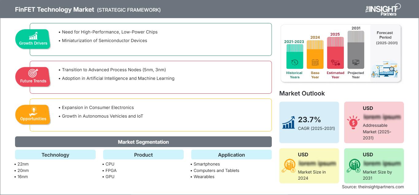
FinFET 기술 시장: 전략적 통찰력
-
이 보고서의 주요 주요 시장 동향을 확인하세요.이 무료 샘플에는 시장 동향부터 추정 및 예측에 이르기까지 데이터 분석이 포함됩니다.
Regional Insights
North America FinFET Technology Market
North America accounted for 24–28% of the world's revenues in 2025 and is expected to grow at a CAGR of 18.8–19.6% up to 2034. The FinFET Technology Market share of North America is based on its position regarding CPU, GPU, FPGA, networking, cloud computing, and electronic design automation. WSTS reported 31.4% growth in semiconductor sales in the Americas in 2025, which confirms robust logic and AI demand. Local incentives for manufacturing encourage customers' interest in secure capacity and advanced packaging.
There is plenty of tape-out activity of US fabless companies and hyperscalers, as well as fabrications in the region increase supply options. Canada provides processor IP, AI development, and design expertise, while Mexico facilitates electronics assembly and automotive supply chains. In purchasing decisions, yield, software compatibility, trusted manufacturing, and packaging options are important. NIST controls programs with US$ 50 billion allocated for manufacturing and R&D.
U.S. FinFET Technology Market
The US accounted for 84-88% of North American revenues in 2025 and is expected to register a CAGR of 19.0-19.8% in the 2026-2034 period. Design motivations include AI accelerators, server processors, premium PCs, networking semiconductors, and military electronics. Significant activities exist from Intel Corporation, Qualcomm Technologies, Inc., Arm Holdings plc, and GlobalFoundries Inc., with international foundries expanding their presence locally.
States such as Arizona, New York, Oregon, and Texas are the key pillars in manufacturing, process development, or semiconductor investment. Customers in the US are starting to blend FinFET compute tiles with packaging and memory to tackle throughput issues with respect to AI without depending exclusively on scaling. The automotive market stresses functional safety and longevity of the supply chain, whereas cloud companies stress performance per watt. According to GAO, 49 semiconductor projects had been funded by July 2026.
Europe FinFET Technology Market
Europe had 11–15% market share in 2025 and would have a 17.4-18.2% CAGR until 2034, with German automobile, industry, and telecom suppliers having demand for qualified processors and controllers with a long lifecycle. The UK provides design expertise, architectures, licenses, and AI. Its fabless industry can be linked seamlessly to foundry and outsourced packaging suppliers worldwide.
French markets include aeronautics, defense, telecommunication, and research; Italian markets include automotive electronics and industrial automation; Spain is working to develop design and digital infrastructure capabilities. According to the European Commission, the initial Chips Act generated more than €52 billion in funding from both public and private sectors. The regional opportunities lie not in duplicating the entire manufacturing base of Asia but in creating design-to-package ecosystems for automotive-grade nodes, secure processors, chiplets, and pilot lines.
APAC FinFET Technology Market
Asia Pacific accounted for 56–60% market share in 2025 and is expected to achieve a 21.2–22.0% CAGR through 2034, making it the leading and fastest growing region. Advanced foundry is dominated by Taiwan, South Korea combines logic and memory, China develops its own design and manufacturing capability, and Japan provides the material, equipment, automotive application, and research.
India is developing design, assembly, and fabrication capabilities, and Australia offers research and data-center demand. Industrial policy, electronics export, smartphones manufacturing, and AI infrastructure will keep the region moving forward. According to WSTS, the semiconductor sales increased by 45.4% in Asia Pacific as well as other regions in 2025.
Middle East & Africa FinFET Technology Market
Market growth in MEA and Africa is forecasted at 15.2% to 16.0% CAGR to 2034. UAE dominates through hyperscale data center capacity, AI programs, advanced connectivity and sovereignty of technology investments. Saudi Arabia supplements by adding cloud computing, smart city and industry digitalization projects while South Africa contributes through telecommunication, finance computation, vehicle assembly and university-based research.
MEA & Rest of demand is expected to remain import-driven and focused on premium products as opposed to semiconductor wafer fabrication. Diversification of energy production and digital infrastructure drives demand for processing, networking chips and automotive controllers. Success factors include distribution coverage, supply security, cyber security and technical enablement for regional OEMs.
Segmentation Analysis
Technology
Technology is projected to expand at a 20.0–20.8% CAGR during 2026–2034. The FinFET Technology Market scope spans cost-optimized 22nm and 20nm options through dense 7nm platforms, permitting buyers to match performance, power, IP maturity, yield, and qualification needs. Node migration is selective: premium compute concentrates at smaller geometries, while automotive, networking, and embedded products extend established process lifecycles.
- 22nm: Established economics, mature design libraries, and balanced power performance support embedded computing, communications, and cost-sensitive products requiring dependable supply and controlled nonrecurring engineering expense.
- 20nm: This node occupies a transitional position between planar scaling and later FinFET generations, with demand concentrated in qualified legacy designs where redesign costs outweigh migration benefits.
- 16nm: Broad foundry availability and proven IP sustain networking, consumer, FPGA, and automotive programs that need strong performance without the mask cost of smaller geometries.
- 14nm: High-volume maturity supports CPUs, controllers, infrastructure, and differentiated applications, while extended qualification and process variants make the node strategically important for long-life products.
- 10nm: Enhanced density and energy efficiency serve mobile, compute, and networking designs, although concentrated manufacturing capability and demanding verification can limit adoption among smaller developers.
- 7nm: Leading revenue contribution comes from GPUs, CPUs, premium mobile processors, and network accelerators, where transistor density and performance per watt justify greater design and wafer costs.
Product
Product is forecast to grow at a 20.2–21.0% CAGR through 2034. CPU demand remains broad across client and server systems, while GPU expansion is accelerated by parallel AI computation. FPGA adoption reflects reconfigurable acceleration and communications needs; MCU migration is more selective because cost, embedded memory, analog integration, and qualification frequently favor mature processes. Product choice therefore determines node economics and packaging intensity.
- CPU: Client, server, and edge processors use FinFETs to balance frequency, density, leakage, and thermal limits, sustaining substantial demand across computing architectures and price tiers.
- FPGA: Reconfigurable devices benefit from dense logic, transceivers, and lower power, supporting telecommunications, industrial control, aerospace, prototyping, and adaptable acceleration where flexibility offsets premium cost.
- GPU: Parallel compute requirements in AI, visualization, gaming, and analytics make GPUs the high-growth product, prioritizing transistor density, bandwidth, chiplets, and advanced packaging.
- MCU: FinFET-based microcontrollers target higher-performance automotive and connected applications, although adoption depends on embedded memory compatibility, safety qualification, mixed-signal integration, and long supply commitments.
Application
Application is expected to expand at a 20.3–21.1% CAGR during 2026–2034. Smartphones established high-volume adoption, while computers, tablets, and networks sustain advanced logic demand. Wearables prioritize leakage control and integration; automotive platforms require functional safety, deterministic performance, and longevity. Across applications, procurement increasingly evaluates total system power, software support, packaging, security, and assured wafer access alongside processor specifications.
- Smartphones: Premium and upper-midrange devices remain major volume users, combining application processors, graphics, modems, and AI engines under strict battery, thermal, and footprint constraints.
- Computers and Tablets: Client systems require efficient CPUs and GPUs for AI-assisted productivity, gaming, and mobility, supporting continuing node migration alongside differentiated mature FinFET platforms.
- Wearables: Always-on sensing, connectivity, and edge inference favor low leakage and compact integration, but small volumes and battery constraints make optimized platform economics essential.
- High-End Networks: Routers, switches, accelerators, and baseband systems demand throughput, transceiver integration, and reliability, making FinFET technology strategically important for cloud and carrier infrastructure.
- Automotive: Software-defined vehicles increase compute for driver assistance, infotainment, connectivity, and centralized control, while qualification, cybersecurity, and decade-long availability shape foundry and node choices.
Opportunity Snapshot
|
Application |
Revenue Contribution |
Trend Tag |
Adoption Stage |
|
Smartphones |
High |
On-device AI |
Mature |
|
Computers and Tablets |
High |
AI PCs |
Scaling |
|
Wearables |
Low |
Always-on Sensing |
Emerging |
|
High-End Networks |
High |
AI Fabric |
Scaling |
|
Automotive |
Medium |
Central Compute |
Scaling |
FinFET Technology Market Growth Drivers and Impact Analysis
Inference, training, and data transfers are driving trends for higher transistor counts in processors, whereas data centers are constrained by their energy, cooling, and density limits. FinFET-based chips support higher density CPU, GPU, and networking silicon with less leakage compared to planar solutions, providing higher useful computation in a given thermal budget. WSTS noted computer applications as the primary driver of the increase in semiconductor volume in 2025 by more than 60% year over year. This will drive wafer productivity, packaging innovation, and reusable IP development. It does not only matter to hyperscale operators since AI personal computers, telecommunications equipment, industry, and edge computing devices need local inference capability.
Connected vehicles expand qualified logic content
Software-defined vehicles are consolidating cockpit, driver-assistance, connectivity, and domain-control workloads onto more capable processors. FinFET nodes provide the compute density needed for sensor fusion and graphics while controlling leakage in thermally constrained electronic control units. Automotive adoption has a distinctive commercial impact: chips require functional-safety evidence, extended temperature support, cybersecurity, and supply commitments lasting far longer than consumer product cycles. These requirements increase qualification cost but create durable design positions once platforms enter production. Foundries and designers that combine automotive-grade libraries, traceable manufacturing, and long-term capacity can secure stable volumes. Demand also spreads across vehicle tiers as centralized architectures move from premium models into broader production.
Policy-backed capacity improves supply resilience
Semiconductor shortages and geopolitical concentration have made fabrication location a board-level sourcing issue. Public programs in the US, Europe, Japan, India, and South Korea reduce selected investment barriers for fabs, packaging, research, and workforce development. NIST’s CHIPS programs allocate US$ 39 billion to manufacturing incentives and US$ 11 billion to research and development, while European initiatives have mobilized more than €52 billion in public and private investment. For FinFET suppliers, the impact is broader regional qualification, more packaging options, and closer customer support. However, incentives cannot remove yield, talent, water, energy, and supplier constraints, so commercially viable projects still require anchor customers, phased ramps, and disciplined utilization planning.
FinFET Technology Market Future Trends
FinFET and gate-all-around portfolios converge
FinFET Technology Market trends will be shaped by a portfolio transition rather than abrupt replacement. Gate-all-around processes will capture the most demanding leading-edge designs, while 7nm, 10nm, 14nm, and 16nm FinFET platforms continue serving products where yield, IP maturity, cost, and qualification outweigh maximum density. Foundries will refine these nodes with lower-voltage libraries, radio-frequency options, automotive reliability, and advanced packaging interfaces. Designers will partition systems so compute-intensive tiles use newer transistors while I/O and control functions remain on proven FinFET processes. This coexistence extends asset lives, widens customer choice, and shifts competition from node labels toward system-level economics.
Chiplet design becomes the scaling default
Chiplets will allow product companies to combine FinFET compute dies with memory, analog, radio-frequency, and I/O components fabricated on different processes. Standardized die-to-die interfaces and package-level design tools will reduce dependence on a single monolithic node, although thermal management, known-good-die testing, and supply coordination become more complex. Foundries and IP providers can differentiate through validated interface blocks, package reference flows, and predictable multi-die yields. The approach is especially relevant for AI accelerators, servers, networking, and automotive domain controllers, where modular reuse shortens development cycles. Over time, platform value will migrate toward co-optimized silicon, interconnect, packaging, and software ecosystems.
FinFET Technology Market Opportunities
Automotive-grade platform expansion
Foundries, IP vendors, and design-service companies can invest in certified FinFET platforms for centralized compute, radar processing, connectivity, and safety controllers. The addressable opportunity extends beyond wafers to functional-safety documentation, secure boot, diagnostics, long-life libraries, and package qualification. Commercial programs should secure anchor vehicle platforms, define decade-scale supply terms, and align node choices with thermal and reliability requirements before capacity commitments. Partnerships with established automotive suppliers reduce qualification risk and shorten customer access. Investors should favor reusable platforms that can serve several vehicle tiers and regions, because fragmented one-off designs may not recover verification expense despite attractive unit economics.
Regional design enablement and secure supply
Emerging semiconductor hubs in the FinFET Technology Market need more than fabrication incentives; they require verified IP, physical-design services, testing, packaging, and engineers capable of converting concepts into manufacturable products. Companies can establish regional design centers around mature FinFET nodes, offering reference flows for industrial, networking, government, and automotive customers. Revenue can combine licensing, engineering fees, prototype runs, and committed production. Action plans should prioritize interoperable tools, export-control compliance, cybersecurity, and partnerships with universities or packaging providers. This opportunity is strongest where customers value trusted supply and customization but lack resources for leading-edge development, allowing established processes to capture differentiated, defensible programs.
Recent Developments
- May 2026: United Microelectronics Corporation (UMC) has introduced a new 14nm embedded high-voltage (eHV) FinFET process platform designed specifically for display driver ICs. The company has made the associated process design kit (PDK) available for customer development following successful validation at its Fab 12A.
- May 2023: Eindhoven, Netherlands / Hsinchu, Taiwan: NXP Semiconductors and TSMC have collaborated to develop what they describe as the automotive industry's first embedded MRAM technology based on 16nm FinFET. The technology is intended to support the next generation of automotive processors and the industry's shift toward software-defined vehicles (SDVs).
- February 2024: Thalia Design Automation has released AMALIA 24.1, the latest version of its platform for semiconductor IP reuse, migration and optimization. The update adds support for 12nm FinFET technology, simulation comparisons for circuit porting, and a new summary-reporting capability within its Technology Analyzer tool.
Frequently Asked Questions

나빈은 맞춤형, 신디케이트 및 컨설팅 프로젝트 전반에 걸쳐 9년 이상의 전문 지식을 보유한 시장 조사 및 컨설팅 전문가입니다. 현재 부사장으로 재직 중이며, 프로젝트 가치 사슬 전반의 이해관계자들을 성공적으로 관리해 왔으며, 100편 이상의 연구 보고서와 30건 이상의 컨설팅 업무를 수행했습니다. 그는 산업 및 정부 프로젝트 전반에 걸쳐 다양한 업무를 수행하며 고객 성공과 데이터 기반 의사 결정에 크게 기여하고 있습니다.
나빈은 카르나타카주 VTU에서 전자통신 공학 학위를, 마니팔 대학교에서 마케팅 및 운영 MBA를 취득했습니다. 그는 9년 동안 IEEE 회원으로 활발하게 활동하며 컨퍼런스, 기술 심포지엄에 참여하고 지역 및 지역 차원에서 자원봉사 활동을 해왔습니다. 현재 직책을 맡기 전에는 IndustryARC에서 준전략 컨설턴트로, 휴렛팩커드(HP Global)에서 산업용 서버 컨설턴트로 근무했습니다.
- 포괄적인 시장 규모 산정 및 전망 분석
- 상세 시장 세분화 분석
- 심층적인 시장 동향 및 요인 분석
- 지역 및 국가별 인사이트
- 경쟁 구도 및 기업 벤치마킹
- 전략적 비즈니스 인텔리전스
사용 후기

The Insight Partners는 당사의 글로벌 시장 진출 전략을 뒷받침하는 가치 있는 시장 정보를 제공했습니다. 담당 팀은 전문적이고 신속하게 대응했으며 당사의 의견을 세심하게 반영했습니다. 또한 프로젝트 전반에 걸쳐 깊이 있는 분석과 유용한 방법론적 설명을 제공했습니다.
Junmo Kim 최고재무책임자(CFO), Enertech Co., Ltd.
Insight Partners의 SCADA 시스템 시장 보고서는 포괄적이며, 현재 동향과 미래 전망에 대한 귀중한 통찰력을 제공합니다. 팀은 매우 전문적이고, 신속하게 대응하며, 처음부터 끝까지 지원해 주었습니다. 저희는 매우 만족하며 Insight Partners의 서비스를 적극 추천합니다.
란 케뎀 파트너, Reali Technologies LTDs
아주 구체적인 소프트웨어 시장에 대한 보고서를 요청했는데, 팀에서 며칠 만에 보고서를 작성해 주셨습니다. 정보는 매우 관련성이 높고 잘 정리되어 있었습니다. 그 후 보고서에 몇 가지 수정과 추가 사항을 요청했습니다. 팀원들의 응답도 매우 빨랐고, 일주일도 채 되지 않아 최종 보고서를 받았습니다.
장-에르브 젠 의장, 퓨처 애널리티카
The Insight Partners와 함께 중요한 시장 조사 및 예측 작업을 진행했습니다. Insight Partners는 기회와 위험에 대한 명확한 통찰력을 제공하여 계획을 세우는 데 큰 도움이 되었습니다. The Insight Partners의 조사는 사용하기 쉬웠고, 탄탄한 데이터를 기반으로 했습니다. 덕분에 현명하고 자신 있는 결정을 내릴 수 있었습니다. The Insight Partners를 강력 추천합니다.
피유시 나그팔 수석 부사장, 하이빔 글로벌
Insight Partners는 탄탄한 분야 전문성을 바탕으로 통찰력 있고 체계적인 시장 조사를 제공했습니다. Insight Partners 팀은 처음부터 끝까지 전문적이고 신속하게 대응했습니다. 사용자 친화적인 웹사이트 덕분에 업계 보고서에 쉽게 접근할 수 있었습니다. 신뢰할 수 있고 고품질의 조사 서비스를 원하신다면 Insight Partners를 강력 추천합니다.
아다치 유키히코 대표이사, 딥블루 주식회사
The Insight Partners에서 시장 보고서를 구매한 것은 이번이 처음입니다. 처음에는 확신이 없었지만, 웹사이트를 방문하고 나서 위험을 감수하고 시장 보고서를 구매하는 것이 더 편하다는 것을 알게 되었습니다. 보고서의 품질과 고객 서비스에 매우 만족합니다. 처음 보고서를 보고 몇 가지 질문과 의견이 있었지만, 분석가와 이메일로 몇 차례 대화를 나눈 후, 전략 기획 과정에 참고할 수 있는 보고서를 확보했다고 생각합니다. 시간을 내어 긍정적인 경험을 선사해 주셔서 정말 감사합니다. 다른 사람들에게도 귀사의 서비스를 적극 추천할 것이며, 추가적인 시장 데이터가 필요할 때면 가장 먼저 귀사에 연락하겠습니다.
존 스즈키 사장 겸 최고 경영자, 이사회 이사, BK 테크놀로지스
나이지리아 감염성 질환 IVD 시장 관련 정보 요청에 응해 주신 귀사의 지원과 전문성에 감사드립니다. 귀사의 인내심과 지도, 그리고 할인 혜택을 기꺼이 제공해 주셔서 결국 계약을 성사시킬 수 있었습니다. 첫 만남을 통해 귀사가 저에게 심어주신 좋은 인상을 바탕으로 앞으로도 The Insight Partners와 함께할 수 있기를 기대합니다.
치지오케 박사 오니아 전무이사, 파인크레스트 헬스케어 유한회사구매 이유
- 정보에 기반한 의사 결정
- 시장 역학 이해
- 경쟁 분석
- 고객 인사이트
- 시장 예측
- 위험 완화
- 전략 기획
- 투자 타당성 분석
- 신흥 시장 파악
- 마케팅 전략 강화
- 운영 효율성 향상
- 규제 동향에 발맞춰 대응




















 무료 샘플 받기 -