Metrología e inspección de semiconductores Crecimiento del mercado, tamaño, participación, tendencias, análisis de actores clave y pronóstico hasta 2028
Datos históricos : | Año base : | Período de pronóstico :Metrología e inspección de semiconductores Crecimiento del mercado, tamaño, participación, tendencias, análisis de actores clave y pronósticos hasta 2028
- Estado : Publicada
- Código de informe : TIPRE00004996
- Categoría : Electrónica y semiconductores
- Número de páginas : 150
- Formatos de informe disponibles :


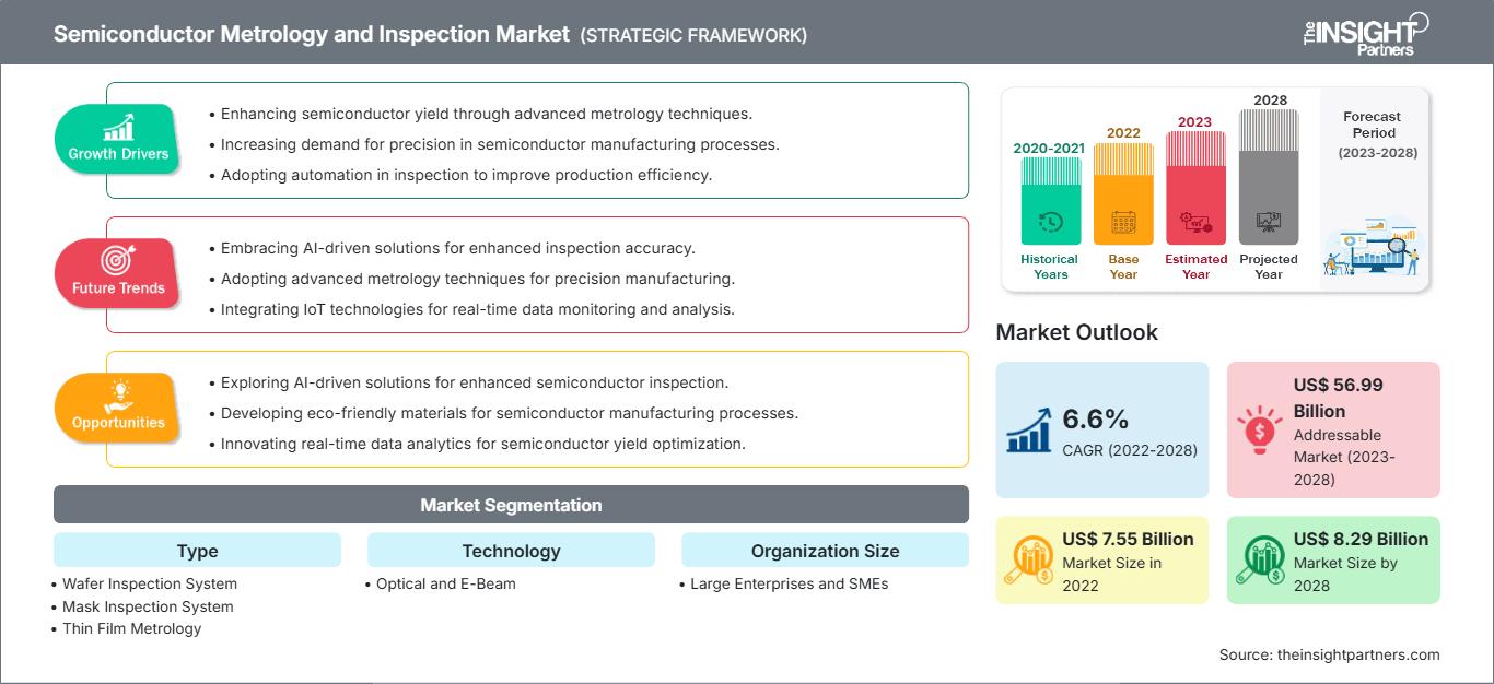
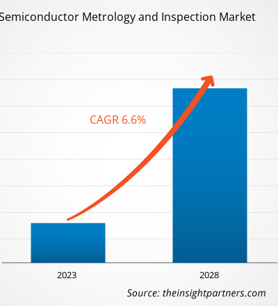
Se proyecta que el mercado de metrología e inspección de semiconductores alcance los US$ 7.553,00 millones en 2022 y los US$ 8.288,55 millones en 2028; se espera que crezca a una CAGR del 6,6% entre 2022 y 2028.
La industria de los semiconductores ha experimentado cambios drásticos a lo largo de los años, que han dado lugar a complejas líneas de montaje para su fabricación. La creciente aplicación de dispositivos inteligentes, el aumento de la automatización industrial y la integración generalizada de chips en vehículos impulsan la demanda global de semiconductores. La inspección de obleas y máscaras, así como otros sistemas de metrología e inspección, se utilizan en la inspección de semiconductores en las líneas de producción; estos sistemas detectan defectos y garantizan la calidad de los dispositivos semiconductores fabricados. Debido a la creciente demanda de semiconductores, los fabricantes se centran en la expansión de sus instalaciones de fabricación, lo que ha impulsado la creciente aplicación de sistemas de metrología e inspección de semiconductores. La mayoría de las empresas están lanzando productos innovadores al mercado. Por ejemplo, Hitachi High-Tech Corporation presentó el SEM*1 CR7300, un nuevo tipo de SEM de revisión que ayudará a mejorar la productividad en la fabricación de dispositivos semiconductores. Se basa en la óptica electrónica, lo que permite la mejor adquisición de imágenes de alta resolución. Simultáneamente, las nuevas tecnologías de imagen y platina permiten la adquisición de imágenes a alta velocidad en la mitad del tiempo que los métodos tradicionales, reduciendo considerablemente el tiempo total de inspección. En 2022, ASML anunció la instalación exitosa de un equipo HMI eScan 1100, el primer sistema de inspección de obleas multihaz para aplicaciones de mejora del rendimiento en línea, como la inspección de defectos por contraste de voltaje y la inspección de defectos físicos. Se espera que las iniciativas mencionadas generen oportunidades para los actores del mercado de metrología e inspección de semiconductores durante el período de pronóstico.
Obtendrá personalización en cualquier informe, sin cargo, incluidas partes de este informe o análisis a nivel de país, paquete de datos de Excel, así como también grandes ofertas y descuentos para empresas emergentes y universidades.
Mercado de metrología e inspección de semiconductores: perspectivas estratégicas
-
Obtenga las principales tendencias clave del mercado de este informe.Esta muestra GRATUITA incluirá análisis de datos, desde tendencias del mercado hasta estimaciones y pronósticos.
Impacto de la pandemia de COVID-19 en los actores del mercado de metrología e inspección de semiconductores
El continuo crecimiento en el número de pacientes infectados por el nuevo coronavirus obligó a las autoridades gubernamentales a imponer confinamientos estrictos en Estados Unidos y otras regiones durante los tres primeros trimestres de 2020. El sector manufacturero sufrió graves pérdidas debido al cierre temporal de fábricas y a los bajos volúmenes de producción, lo que obstaculizó el crecimiento de los sectores automotriz, de electrónica y semiconductores, y minorista. Los efectos de la pandemia de COVID-19 redujeron el tamaño del mercado norteamericano de metrología e inspección de semiconductores durante los tres primeros trimestres de 2020. Además, las medidas de confinamiento provocaron una interrupción masiva en la cadena de suministro en toda la región, lo que desencadenó una enorme acumulación de pedidos y provocó la pérdida de ingresos para muchas empresas grandes y pequeñas que operan en el mercado norteamericano de metrología e inspección de semiconductores. Sin embargo, el mercado experimentó un impacto positivo desde el cuarto trimestre de 2020. La escasez de semiconductores, debido a las interrupciones causadas por la pandemia, obligó a los fabricantes a optimizar el uso de sus materias primas, lo que condujo a una mayor inversión en la adquisición de estos equipos, impulsando así el tamaño del mercado de metrología e inspección de semiconductores. Esto permitió a los actores del mercado generar ingresos y contribuir al crecimiento del mercado de metrología e inspección de semiconductores. No obstante, los ingresos generados en 2020 fueron ligeramente inferiores a los generados en 2019, pero crecieron sustancialmente en 2021. Por lo tanto, aunque la pandemia causó ciertas interrupciones, los negocios de los actores de metrología e inspección de semiconductores se vieron afectados positivamente debido a la pandemia.
Perspectivas del mercado de metrología e inspección de semiconductores
Las tecnologías de empaquetado avanzado (PA) desempeñan un papel cada vez más crucial en la fabricación de obleas, la manufactura y los procesos de semiconductores asociados. Con la creciente complejidad de las arquitecturas de dispositivos y el impulso a la integración heterogénea, el PA se ha convertido en un factor clave para la mejora del rendimiento y la miniaturización. Estos avances han influido significativamente en el panorama de la demanda de herramientas de metrología e inspección de semiconductores, especialmente en entornos de fabricación back-end. El control preciso de diversos procesos es esencial para garantizar la fiabilidad y el rendimiento de los dispositivos empaquetados avanzados. A diferencia de los procesos de semiconductores front-end, el PA presenta desafíos únicos para la metrología y la inspección debido a la naturaleza no plana y multicapa de las estructuras de empaquetado avanzado. Problemas como la variación de la altura de las protuberancias, la detección de huecos, la desalineación y los defectos subsuperficiales no visibles exigen soluciones de inspección especializadas. Además, la diversidad de materiales, que abarca desde vías a través del silicio (TSV) hasta la integración de chips y chips, requiere técnicas de metrología altamente adaptables y avanzadas para garantizar un control de calidad sólido. Las técnicas de inspección y medición son fundamentales para gestionar el rendimiento, identificar defectos y mantener la uniformidad del proceso. Con la miniaturización de los tamaños de las características y el aumento de la complejidad en las estructuras de interconexión, la industria de los semiconductores es testigo de una mayor necesidad de sistemas de metrología que ofrezcan una precisión excepcional, alta sensibilidad y optimización del rendimiento.
La creciente complejidad y personalización inherentes a la AP impulsan la innovación en tecnologías de inspección, como la metrología óptica 3D, la inspección por rayos X y los sistemas de imágenes infrarrojas. Estas herramientas son esenciales para el desarrollo y la optimización de procesos en diversos formatos de AP, además de su importante papel en la detección de defectos. Como resultado, el mercado de metrología e inspección de semiconductores experimenta un crecimiento sostenido, impulsado por la continua evolución de las tecnologías de AP.
La aceleración de las aplicaciones de IA, 5G y computación de alto rendimiento está intensificando la demanda de interconexiones de alta densidad y formatos avanzados, lo que a su vez impulsa la dependencia de AP. Esto, a su vez, genera sólidas oportunidades de crecimiento para los proveedores de soluciones de metrología e inspección capaces de satisfacer las exigentes demandas del encapsulado de semiconductores de próxima generación.
Perspectivas basadas en el tamaño de la organización
El mercado de metrología e inspección de semiconductores, por tamaño de organización, se segmenta en grandes empresas y pymes (pequeñas y medianas empresas). Se espera que el segmento de grandes empresas registre una tasa de crecimiento anual compuesta (TCAC) más alta durante el período de pronóstico. Las grandes empresas son los principales usuarios finales del mercado. Esto incluye fundiciones como TSMC y GlobalFoundry, y fabricantes de dispositivos integrados como Intel Corporation y Samsung Corporation. En noviembre de 2021, Samsung Corporation anunció la construcción de una unidad de fabricación de semiconductores en Texas debido a la creciente demanda de chips para teléfonos y otros dispositivos. La compañía planeó invertir US$17 mil millones en la construcción de esta unidad. Se espera que una parte significativa de esa cantidad se utilice para la compra de equipos de metrología e inspección de semiconductores. Se espera que estos desarrollos estratégicos adoptados por las grandes empresas impulsen el crecimiento del mercado de metrología e inspección de semiconductores para este segmento durante el período de pronóstico.
El mercado de metrología e inspección de semiconductores está segmentado según el tipo, la tecnología, el tamaño de la organización y la geografía.
- Según el tipo, el mercado está segmentado en sistema de inspección de obleas, sistema de inspección de máscara, metrología de película delgada, inspección de golpes, inspección de paquetes, inspección de marcos conductores e inspección de tarjetas de sonda.
- Según la tecnología, el mercado de metrología e inspección de semiconductores está segmentado en óptico y de haz electrónico.
- Por tamaño de organización, el mercado se bifurca en grandes empresas y PYMES.
- Según la geografía, el mercado de inspección y metrología de semiconductores está segmentado principalmente en América del Norte, Europa, Asia Pacífico (APAC) y el resto del mundo (ROW).
Entre los actores clave que operan en el mercado se encuentran KLA Corporation; ASML Holding NV; Applied Materials, Inc.; Onto Innovation, Inc.; y Hitachi High-Technologies Corporation.
Perspectivas regionales del mercado de metrología e inspección de semiconductores
Los analistas de The Insight Partners han explicado detalladamente las tendencias y los factores regionales que influyen en el mercado de metrología e inspección de semiconductores durante el período de pronóstico. Esta sección también analiza los segmentos y la geografía del mercado de metrología e inspección de semiconductores en Norteamérica, Europa, Asia Pacífico, Oriente Medio y África, y Sudamérica y Centroamérica.
Alcance del informe de mercado de metrología e inspección de semiconductores
| Atributo del informe | Detalles |
|---|---|
| Tamaño del mercado en 2022 | 7.550 millones de dólares estadounidenses |
| Tamaño del mercado en 2028 | US$ 8.29 mil millones |
| CAGR global (2022-2028) | 6,6% |
| Datos históricos | 2020-2021 |
| Período de pronóstico | 2023-2028 |
| Segmentos cubiertos |
Por tipo
|
| Regiones y países cubiertos |
América del norte
|
| Líderes del mercado y perfiles de empresas clave |
|
Densidad de actores del mercado de metrología e inspección de semiconductores: comprensión de su impacto en la dinámica empresarial
El mercado de metrología e inspección de semiconductores está creciendo rápidamente, impulsado por la creciente demanda de los usuarios finales debido a factores como la evolución de las preferencias de los consumidores, los avances tecnológicos y un mayor conocimiento de las ventajas del producto. A medida que aumenta la demanda, las empresas amplían su oferta, innovan para satisfacer las necesidades de los consumidores y aprovechan las tendencias emergentes, lo que impulsa aún más el crecimiento del mercado.
- Obtenga una descripción general de los principales actores clave del mercado de metrología e inspección de semiconductores
En el mercado de metrología e inspección de semiconductores, las empresas se centran principalmente en el desarrollo de productos avanzados y eficientes.
- En 2022, Lasertec Corporation anunció el lanzamiento de la serie MATRICS X9ULTRA, un sistema de inspección de máscaras diseñado para inspeccionar las fotomáscaras utilizadas en la litografía ultravioleta extrema (EUV) mientras sus películas no están adheridas.
- En 2020, KLA Corporation anunció dos nuevos productos: el sistema de geometría de obleas PWG5 y el sistema de inspección de defectos de obleas Surfscan SP7XP. Estos nuevos sistemas están diseñados para abordar problemas extremadamente complejos en la fabricación de circuitos integrados de memoria y lógica de vanguardia.

Naveen es un experimentado profesional en investigación de mercados y consultoría con más de 9 años de experiencia en proyectos personalizados, sindicados y de consultoría. Actualmente se desempeña como Vicepresidente Asociado, donde ha gestionado con éxito a las partes interesadas en toda la cadena de valor del proyecto y ha redactado más de 100 informes de investigación y más de 30 proyectos de consultoría. Su trabajo abarca proyectos industriales y gubernamentales, contribuyendo significativamente al éxito de los clientes y a la toma de decisiones basada en datos.
Naveen es licenciado en Ingeniería Electrónica y Comunicaciones por la VTU (Karnataka) y tiene un MBA en Marketing y Operaciones por la Universidad de Manipal. Ha sido miembro activo del IEEE durante 9 años, participando en conferencias, simposios técnicos y realizando voluntariado tanto a nivel de sección como regional. Antes de su puesto actual, trabajó como Consultor Estratégico Asociado en IndustryARC y como Consultor de Servidores Industriales en Hewlett Packard (HP Global).
- Análisis histórico (2 años), año base, pronóstico (7 años) con CAGR
- Análisis PEST y FODA
- Tamaño del mercado, valor/volumen: global, regional y nacional
- Industria y panorama competitivo
- Conjunto de datos de Excel
Testimonios
El informe de mercado de sistemas SCADA de Insight Partners es completo y ofrece información valiosa sobre las tendencias actuales y las previsiones futuras. El equipo fue altamente profesional, receptivo y me brindó un gran apoyo en todo momento. Estamos muy satisfechos y recomendamos ampliamente sus servicios.
RAN KEDEM Socio, Reali Technologies LTDsSolicité un informe sobre un mercado de software muy específico y el equipo lo elaboró en pocos días. La información era muy relevante y estaba bien presentada. Posteriormente, solicité algunos cambios y adiciones al informe. El equipo fue muy receptivo y recibí el informe final en menos de una semana.
JEAN-HERVE JENN Presidente, Future AnalyticaTrabajamos con The Insight Partners para un importante estudio y pronóstico de mercado. Nos brindaron una visión clara de las oportunidades y los riesgos, lo que nos ayudó a definir nuestros planes. Su investigación fue fácil de usar y se basó en datos sólidos. Nos ayudó a tomar decisiones inteligentes y seguras. Los recomendamos ampliamente.
PIYUSH NAGPAL Vicepresidente Sénior, , High Beam GlobalThe Insight Partners realizó una investigación de mercado profunda y bien estructurada con una sólida experiencia en el sector. Su equipo fue profesional y receptivo en todo momento. El sitio web, fácil de usar, facilitó el acceso a los informes del sector. Los recomendamos ampliamente por sus servicios de investigación confiables y de alta calidad.
YUKIHIKO ADACHI Director Ejecutivo, , Deep Blue, LLCEsta es la primera vez que compro un informe de mercado de The Insight Partners. Aunque al principio tenía dudas, visité su sitio web y me sentí más cómodo al arriesgarme y comprarlo. Estoy completamente satisfecho con la calidad del informe y el servicio al cliente. Tenía varias preguntas y comentarios sobre el informe inicial, pero después de un par de conversaciones por correo electrónico con su analista, creo que tengo un informe que puedo usar como base para nuestro proceso de planificación estratégica. Muchas gracias por tomarse el tiempo y hacer de esta una experiencia positiva. Sin duda, recomendaré sus servicios y serán mi primera opción cuando necesitemos más datos de mercado.
JOHN SUZUKI Presidente y Director Ejecutivo, Director de la Junta Directiva, BK TechnologiesAgradezco su apoyo y la profesionalidad que demostraron al atender mi solicitud de información sobre el mercado de diagnóstico in vitro (IVD) para enfermedades infecciosas en Nigeria. Agradezco su paciencia, su orientación y su disposición a ofrecerme un descuento, lo que finalmente nos permitió cerrar un trato. Espero poder colaborar con The Insight Partners en el futuro, gracias a la impresión que me causó este primer encuentro.
DRA. CHIJIOKE ONYIA, DIRECTORA GENERAL, PineCrest Healthcare Ltd.Razón para comprar
- Toma de decisiones informada
- Comprensión de la dinámica del mercado
- Análisis competitivo
- Información sobre clientes
- Pronósticos del mercado
- Mitigación de riesgos
- Planificación estratégica
- Justificación de la inversión
- Identificación de mercados emergentes
- Mejora de las estrategias de marketing
- Impulso de la eficiencia operativa
- Alineación con las tendencias regulatorias


Desbloquea descuentos exclusivos en informes
Consultar ahora


 Obtenga una muestra gratuita para - Mercado de metrología e inspección de semiconductores