
Electronic Board Level Underfill and Encapsulation Material Market Share, Size & Demand by 2034
Coverage: By Product Type (Underfills, Gob Top Encapsulations); Material (Quartz/Silicone, Alumina-based, Epoxy -based, Urethane -based, Acrylic -based, Others); Board Type (CSP (Chip Scale Packages), BGA (Ball Grid Arrays), Flip Chips) , and Geography (North America, Europe, Asia Pacific, and South and Central America)
- Status : Data Released
- Report Code : TIPRE00017574
- Category : Chemicals and Materials
- No. of Pages : 150
- Available Report Formats :


- Last update date : September 30, 2026


2025 Market Size
US$ 368.8 Mn
Base year value
2034 Forecast
US$ 543.65 Mn
Projected by 2034
CAGR 2026-2034
4.41 %
Growth rate
Addressable Market
US$ 4,144.16 Mn
(2026-2034)
The Electronic Board Level Underfill and Encapsulation Material Market size was valued at US$ 368.8 Million in 2025 and is projected to reach US$ 543.65 Million by 2034, registering a CAGR of 4.41% during 2026-2034. The market covers materials used to reinforce and protect electronic interconnections and components at the board level, including underfills and glob top encapsulations formulated from quartz/silicone, alumina-based, epoxy-based, urethane-based, and acrylic-based materials for CSP, BGA, and flip-chip assemblies.
North America represents an important demand center, accounting for a modeled ~28% of the global Electronic Board Level Underfill and Encapsulation Material Market in 2025, with a projected ~3.9% CAGR through 2034. Demand is supported by semiconductor packaging, aerospace and defense electronics, industrial controls, medical electronics, and high-reliability computing equipment. The regional ecosystem benefits from established electronic materials suppliers and advanced packaging capabilities. H.B. Fuller, AI Technology, Parker-Hannifin, and YINCAE maintain portfolios addressing underfill, encapsulation, and related electronic protection requirements.
Electronic Board Level Underfill and Encapsulation Material Market Assessment and Insights
- North America: The region held a modeled ~28% global Electronic Board Level Underfill and Encapsulation Material Market share in 2025 and is expected to record a ~3.9% CAGR. Established semiconductor, electronics manufacturing, aerospace, medical, and defense supply chains support demand for materials combining mechanical reinforcement, thermal-cycle reliability, and process compatibility.
- U.S.: The U.S. represented a modeled ~82% of North American demand in 2025 and is projected to expand at ~3.8% CAGR. Semiconductor packaging development, domestic electronics manufacturing, defense procurement, and advanced PCB assembly support demand for precision underfills and encapsulants.
- Europe: Europe accounted for a modeled ~23% global share in 2025 and is expected to grow at ~4.0% CAGR. Germany, France, Italy, and the UK provide important electronics manufacturing and industrial technology demand. Reliability requirements, automotive electronics, industrial automation, and compliance-oriented material selection differentiate the region.
- Asia Pacific: Asia Pacific represented a modeled ~43% global share in 2025 and is forecast to expand at ~5.3% CAGR. China, Japan, South Korea, Taiwan, and India provide strong industrial foundations through semiconductor packaging, consumer electronics, telecommunications, automotive electronics, and electronics manufacturing services.
- Largest Segment: Underfills are estimated to remain the largest segment and are projected to grow at ~4.3% CAGR during 2026-2034. Their broad use across BGA, CSP, and flip-chip assemblies makes them integral to solder-joint reinforcement and thermal-mechanical reliability.
- High Growth Segment: Flip-chips are projected to record the fastest growth at ~5.3% CAGR. Increasing use of high-density interconnects, advanced semiconductor packages, and compact electronic architectures increases demand for materials capable of filling narrow gaps while controlling stress and warpage.
- Key companies analyzed in detail: AI Technology, Inc.; ASE Technology Holding Co., Ltd.; H.B. Fuller Company; Resonac Corporation; Indium Corporation; Parker-Hannifin Corporation; NAMICS Corporation; Protavic International, Inc.; Dow Inc.; YINCAE Advanced Materials, LLC; Henkel AG & Co. KGaA; Sumitomo Bakelite Co., Ltd.
Source: The Insight Partners' analysis based on proprietary research, government publications, company annual reports, investor presentations, industry databases, and expert interviews.
This market has been shifting from traditional protection materials to formulations based on packaging structure, thermal considerations, processing speed, and increased demand for higher reliability. While conventional epoxy underfills will be significant, differentiation by suppliers will be achieved via low CTE, controllable viscosity, rapid capillary action, low temperature curing, decreased resin bleed, thermal conductivity, optical transparency, and ability to work in no-clean assembly processes.
Package architecture is set to play a greater role as a formulation driver. Greater die sizes, smaller pitches, narrow gaps, and heterogeneous integration will necessitate control of the flow, filler content, shrinkage, adhesion, and curing properties of the materials. The product development efforts are therefore expected to be directed towards application-specific formulations rather than general-purpose electronic adhesives.
Through 2034, material development is anticipated to continue the trend of developing formulations for larger dies, finer pitches, increased heat dissipation needs, and heterogeneous integration. There will be continued expansion of low warpage and thermal conductivity formulations and improvement of automated dispensing properties. Localization of semiconductor packaging industry is another structural factor which has developed, especially with the addition of new packaging capacities in the U.S., Europe, China, South Korea, Japan, Taiwan, and India.
Electronic Board Level Underfill and Encapsulation Material Market Report Scope
| Report Attribute | Details |
|---|---|
| Market size in 2025 | US$ 368.8 Million |
| Market Size by 2034 | US$ 543.65 Million |
| Global CAGR (2026 - 2034) | 4.41% |
| Historical Data | 2021-2024 |
| Forecast period | 2026-2034 |
Electronic Board Level Underfill and Encapsulation Material Market Analysis
The Electronic Board Level Underfill and Encapsulation Material market depends largely on reliability considerations of denser assemblies. Increasing component density translates into increased thermal and mechanical stresses and, hence, the need for material to mitigate solder joint fatigue and interconnection protection. The suppliers of these materials develop their products by optimizing their characteristics including viscosity, filler content, curing cycle, CTE, adhesion, and reworkability for individual assembly process.
The Electronic Board Level Underfill and Encapsulation Material Market report indicates that the value chain for the industry stretches from the resin and inorganic filler suppliers to formulators, dispensing equipment suppliers, semiconductor packaging manufacturers, PCB assemblers, and OEMs. Epoxy resins offer an important base for formulations on account of their adhesion and mechanical attributes, whereas silicone, urethane, acrylic, and filled resins cater to specific needs.
Positioning is now more and more influenced by formulation and performance combinations than by material availability alone. The H.B. Fuller strategy revolves around reliability and reworkability, YINCAE distinguishes itself through its fast flow and thermally conductive formulations, Resonac offers liquid encapsulant formulations for flip-chip and FC-BGA applications, and Parker-Hannifin provides frozen underfill encapsulants which have been optimized to controlled dispensing and cure conditions.
Thus, the Electronic Board Level Underfill and Encapsulation Material assessment suggests a market situation where qualification, application engineering, process suitability, and reliability information are equally significant as the chemistry itself. Formulation companies with wide product lines will be able to cover all possible package designs, while specialization is possible in relation to special properties such as optical clarity, exceptional thermal characteristics, low-temperature cure, or reworkability.
● REPORT CUSTOMIZATION
Tailor This Report To Align With Your Specific Business Requirements
This report can be customized to align precisely with your business objectives, scope, and target markets. Customization options include tailored segmentation, geography, competitive analysis, and strategic insights to support informed decision-making.
Customize This Report →WHAT YOU CAN ADJUST
- ● Segmentations
- ● Geography
- ● Competitive Analysis
- ● Language Preferences
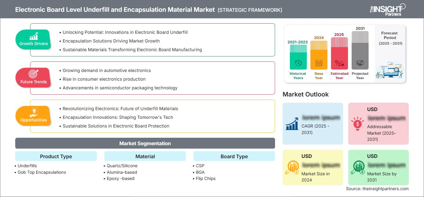
Electronic Board Level Underfill and Encapsulation Material Market: Strategic Insights
Regional Insights
North America Electronic Board Level Underfill and Encapsulation Material Market
North America accounted for a modeled ~28% of the global market in 2025 and is expected to expand at ~3.9% CAGR. The regional market is supported by semiconductor design, advanced packaging, aerospace and defense electronics, medical devices, industrial systems, and high-performance computing. The U.S. represents the dominant demand center, while Canada contributes through specialized electronics, industrial, and resource-sector equipment applications.
Material qualification is particularly important because electronics manufacturers require consistent dispensing behavior, thermal-cycle reliability, moisture resistance, and compatibility with automated assembly. AI Technology and YINCAE maintain dedicated underfill and glob-top portfolios, while H.B. Fuller supplies board-level formulations for CSP, BGA, and flip-chip applications.
U.S. Electronic Board Level Underfill and Encapsulation Material Market
The U.S. represented a modeled ~82% of North American demand in 2025 and is expected to grow at ~3.8% CAGR. Market is benefited by investments made in semiconductors, defense electronics, aerospace, medical devices, telecommunication and high performance computing. Customers are now looking at the properties of the materials in terms of reliability, performance and production efficiencies and not just the adhesive strength.
High precision dispensing technology being available with electronics manufacturers also provides additional impetus. Underfill processes are being incorporated within advanced electronics manufacturing process flows, especially for Flip Chip, BGA, CSP and other high-reliability assembly types.
Europe Electronic Board Level Underfill and Encapsulation Material Market
Europe held a modeled ~23% global share in 2025 and is projected to grow at ~4.0% CAGR. Germany is the most important country because of its automotive electronics, industrial automation, semiconductor equipment, and electronics manufacturing base. France contributes through aerospace, defense, automotive, and industrial electronics, while Italy has substantial industrial automation, power electronics, and specialized machinery demand. The UK adds demand through aerospace, defense, telecommunications, and advanced electronics.
European buyers place strong emphasis on long-term reliability, controlled processing, environmental compliance, and supply-chain continuity. The region's engineering-oriented electronics ecosystem supports demand for formulations that can satisfy specific package, substrate, curing, and reliability requirements.
APAC Electronic Board Level Underfill and Encapsulation Material Market
APAC accounted for a modeled ~43% share in 2025 and is expected to register a ~5.3% CAGR. China offers robust demand in electronics manufacturing, while Japan and South Korea offer semiconductor manufacturing along with material science. The importance of Taiwan lies in its semiconductor foundry and packaging ecosystem, and that of India lies in building up its semiconductor and electronics manufacturing capability.
Semiconductor materials development capabilities lie with Japan, where Resonac and Sumitomo Bakelite provide a broad range of packaging material capabilities. South Korea’s semiconductor manufacturing ecosystem drives the demand for high-reliability underfill and encapsulation materials, while China’s large electronics assembly ecosystem drives the volume demand and localization of such materials. Indian semiconductor ecosystem is building an additional qualification market for packaging materials and equipment.
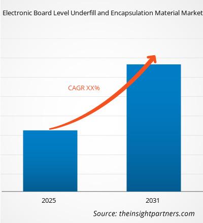
Segmentation Analysis
Product Type
Underfills include materials dispensed beneath semiconductor packages to reinforce solder interconnections, control CTE mismatch, and improve resistance to thermal cycling and mechanical shock. This segment is projected to grow at ~4.3% CAGR and remains the largest because CSP, BGA, and flip-chip assemblies require increasingly controlled interconnect protection. Fast-flow, low-temperature, reworkable, and thermally conductive formulations are becoming more important.
Gob Top Encapsulations cover localized encapsulation of chips and components using dispensed materials that protect sensitive assemblies against moisture, contamination, vibration, and mechanical damage. This segment is projected to grow at ~4.6% CAGR as compact electronics require localized protection without the processing burden of full-package molding.
Material
Quartz/Silicone materials provide flexibility, thermal stability, and stress relief and are particularly relevant where mechanical compliance or optical characteristics are important. This main segment is projected to grow at ~4.8% CAGR.
Alumina-based formulations provide a route toward improved thermal performance while retaining electrical insulation. Their adoption is tied to power-dense electronics and assemblies where heat dissipation is an important reliability consideration. The segment is projected to grow at ~5.0% CAGR.
Epoxy-based materials remain the core formulation category because of strong adhesion, mechanical reinforcement, chemical resistance, and compatibility with established dispensing and curing processes. The segment is projected to grow at ~4.2% CAGR.
Urethane-based formulations provide flexibility and stress accommodation for applications requiring greater compliance. Demand is supported by electronics exposed to vibration, thermal movement, or mechanical shock, with the segment projected to grow at ~4.5% CAGR.
Acrylic-based materials support specialized curing, adhesion, and processing requirements and can be advantageous where rapid processing or particular optical and mechanical characteristics are required. The segment is projected to grow at ~4.0% CAGR.
Board Type
CSP assemblies benefit from underfill reinforcement because compact package geometry leaves limited room for stress dissipation. The segment is projected to grow at ~4.0% CAGR and remains relevant in mobile, consumer, communications, and compact industrial electronics.
BGA is projected to grow at ~4.2% CAGR. Its broad use in computing, industrial electronics, automotive systems, telecommunications, and embedded electronics sustains demand for materials that improve solder-joint reliability and accommodate board-level thermal cycling.
Flip-chip packages are projected to grow at ~5.3% CAGR as high-density packaging, optical devices, and heterogeneous integration increase the use of fine-pitch interconnects. Materials must combine rapid gap filling with low warpage, high adhesion, controlled CTE, and resistance to thermal stress.
Opportunity Snapshot
| Board Type | Revenue Contribution (High/Medium/Low) | Trend Tag | Adoption Stage |
| CSP | Medium | Compact packaging | Mature |
| BGA | High | Reliability reinforcement | Mature |
| Flip Chips | High | Fine-pitch integration | Scaling |
Electronic Board Level Underfill and Encapsulation Material Market Growth Drivers and Impact Analysis
Rising Package Density and Interconnect Reliability Requirements
Higher component density increases mechanical and thermal stress around solder interconnections. Underfills distribute stress away from vulnerable joints and improve resistance to thermal cycling, vibration, shock, and moisture. As packages incorporate finer pitches and larger dies, the process window for material flow becomes narrower, increasing demand for formulations with controlled viscosity, low void formation, and predictable curing.
This driver strengthens demand for materials engineered around specific package architectures. Suppliers that can demonstrate reliable flow, adhesion, curing, and thermal-mechanical performance are better positioned during customer qualification because material selection increasingly influences assembly yield and field reliability.
Expansion of Advanced Semiconductor Packaging
2. xD, 3D, chiplet, and heterogeneous packaging are expanding the role of materials in package reliability. Underfill suppliers must accommodate large package bodies, narrow gaps, fine-pitch connections, and warpage-sensitive structures. Resonac's work on fine-pitch underfill and next-generation package materials illustrates the movement toward materials engineered around advanced packaging architectures rather than generic board assembly.
As semiconductor packaging becomes more structurally complex, material suppliers need closer collaboration with OSATs, foundries, substrate manufacturers, and equipment providers. This creates higher qualification barriers but can strengthen customer relationships once a formulation is integrated into a production process.
Demand for Faster and Lower-Temperature Processing
Electronics manufacturers increasingly seek materials that reduce curing time, processing temperature, and manufacturing complexity without compromising reliability. Fast-flow and snap-cure formulations can improve throughput, while low-temperature materials reduce thermal exposure to sensitive components.
Processing efficiency is consequently becoming an important purchasing criterion alongside material reliability. Suppliers that combine rapid processing with predictable curing and low void formation can address production environments in which cycle time and yield directly influence the economics of advanced electronic assembly.
Electronic Board Level Underfill and Encapsulation Material Market Future Trends
Electronic Board Level Underfill and Encapsulation Material trends toward multifunctional formulations
Material suppliers are increasingly combining mechanical reinforcement with thermal management, optical performance, low warpage, and process simplification. Thermally conductive and optical underfills illustrate the movement from single-purpose protection toward multifunctional materials.
This Electronic Board Level Underfill and Encapsulation Material Market trend is particularly relevant for applications where electrical density and heat generation are increasing simultaneously. Suppliers capable of controlling filler chemistry without sacrificing flow, adhesion, and curing behavior can address more demanding package designs and increase their relevance in advanced semiconductor applications.
Low-Warpage Materials for Larger Packages
Larger semiconductor packages amplify warpage and stress-management challenges. Liquid encapsulants with controlled flow and low shrinkage are therefore gaining strategic importance. Advanced encapsulation development increasingly focuses on package geometry, thermal cycling, stress distribution, and compatibility with larger package bodies.
The trend will influence formulation design, particularly as chiplet architectures and high-performance computing packages increase package dimensions and structural complexity. Material suppliers will need to balance filler loading and thermal performance against viscosity, flow, shrinkage, and manufacturability.
No-Clean and Residue-Compatible Processing
Compatibility between flux residues and underfill materials is becoming increasingly important as manufacturers reduce cleaning operations. Materials must maintain adhesion and reliability despite changes in flux chemistry and surface conditions.
This development encourages closer coordination between flux, underfill, substrate, and dispensing suppliers. It can reduce manufacturing steps while increasing the importance of material compatibility testing during qualification.
Electronic Board Level Underfill and Encapsulation Material Market Opportunities
Advanced Optical and Photonic Packaging
Optical sensors, silicon photonics, MicroLED devices, image sensors, and AR/VR modules create opportunities for underfills that combine mechanical protection with optical transparency. Conventional opaque or highly filled materials can restrict design flexibility in these applications.
Suppliers developing transparent formulations with controlled flow, rapid curing, low stress, and reliable adhesion can address a specialized but expanding application space. The opportunity is particularly relevant to advanced packaging developers in North America and APAC, where semiconductor and photonic manufacturing ecosystems are concentrated.
Localized Material Supply for Emerging Semiconductor Hubs
The expansion of semiconductor packaging in India, the U.S., and other emerging manufacturing locations creates opportunities for regional material qualification, technical support, and localized inventory. Customers increasingly need application engineering alongside material supply because underfill performance depends on dispensing equipment, substrate preparation, flux chemistry, curing profiles, and package geometry.
Suppliers that establish regional technical capabilities can reduce qualification friction and strengthen customer retention. Local formulation support, rapid sampling, application laboratories, and inventory availability can become differentiators as semiconductor supply chains diversify geographically.
Recent Developments
- August 2026: YINCAE Advanced Materials, LLC - YINCAE introduced UF 88UV, a high-transparency optical underfill designed for optical modules, optoelectronic devices, and advanced semiconductor packaging. The material combines room-temperature flow with optical clarity and inspection capability, extending the company's portfolio toward photonics and advanced packaging applications. The launch reinforces the shift toward specialized underfills addressing optical performance alongside mechanical and thermal reliability.
- June 2026: Sumitomo Bakelite Co., Ltd. - Sumitomo Bakelite announced the expansion of production capacity for semiconductor encapsulation materials at its Suzhou operation. The move strengthens regional supply capability for semiconductor packaging materials as advanced packaging demand increases in Asia. Capacity expansion supports localization and supply continuity while positioning the company to serve semiconductor packaging requirements from customers operating within China's manufacturing ecosystem.
Frequently Asked Questions

- Comprehensive Market Sizing and Forecast Analysis
- Detailed Segmentation Analysis
- In-Depth Market Dynamics Assessment
- Regional and Country-Level Insights
- Competitive Landscape and Company Benchmarking
- Strategic Business Intelligence
Recent Reports
Testimonials

The Insight Partners' SCADA System Market report is comprehensive, with valuable insights on current trends and future forecasts. The team was highly professional, responsive, and supportive throughout. We are very satisfied and highly recommend their services.
RAN KEDEM Partner, Reali Technologies LTDs
I requested a report on a very specific software market and the team produced the report in a few days. The information was very relevant and well presented. I then requested some changes and additions to the report. The team was again very responsive and I got the final report in less than a week.
JEAN-HERVE JENN Chairman, Future Analytica
We worked with The Insight Partners for an important market study and forecast. They gave us clear insights into opportunities and risks, which helped shape our plans. Their research was easy to use and based on solid data. It helped us make smart, confident decisions. We highly recommend them.
PIYUSH NAGPAL Sr. Vice President, High Beam Global
The Insight Partners delivered insightful, well-structured market research with strong domain expertise. Their team was professional and responsive throughout. The user-friendly website made accessing industry reports seamless. We highly recommend them for reliable, high-quality research services
YUKIHIKO ADACHI CEO, Deep Blue, LLC.
This is the first time I have purchased a market report from The Insight Partners.While I was unsure at first, I visited their web site and felt more comfortable to take the risk and purchase a market report.I am completely satisfied with the quality of the report and customer service. I had several questions and comments with the initial report, but after a couple of dialogs over email with their analyst I believe I have a report that I can use as input to our strategic planning process.Thank you so much for taking the extra time and making this a positive experience.I will definitely recommend your service to others and you will be my first call when we need further market data.
JOHN SUZUKI President and Chief Executive Officer, Board Director, BK Technologies
I wish to appreciate your support and the professionalism you displayed in the course of attending to my request for information regarding to infectious disease IVD market in Nigeria. I appreciate your patience, your guidance, and the fact that you were willing to offer a discount, which eventually made it possible for us to close a deal. I look forward to engaging The Insight Partners in the future, all thanks to the impression you have created in me as a result of this first encounter.
DR CHIJIOKE ONYIA MANAGING DIRECTOR, PineCrest Healthcare Ltd.Reason to Buy
- Informed Decision-Making
- Understanding Market Dynamics
- Competitive Analysis
- Identifying Emerging Markets
- Customer Insights
- Market Forecasts
- Risk Mitigation
- Boosting Operational Efficiency
- Strategic Planning
- Investment Justification
- Tracking Industry Innovations
- Aligning with Regulatory Trends





 Get Free Sample for