
Semiconductor Capital Equipment Market Share, Size & Demand by 2034
Coverage: By Equipment Type (Automated Test Equipment, Die-Level Packaging and Assembly Equipment, Wafer-Level Manufacturing Equipment); End-User (Memory manufacturers, Foundries, IDMs) , and Geography (North America, Europe, Asia Pacific, and South and Central America)
- Status : Data Released
- Report Code : TIPRE00014539
- Category : Electronics and Semiconductor
- No. of Pages : 150
- Available Report Formats :


- Last update date : July 10, 2026


2025 Market Size
US$ 115.25 Bn
Base year value
2034 Forecast
US$ 259.37 Bn
Projected by 2034
CAGR 2026-2034
9.43 %
Growth rate
Addressable Market
US$ 1,672.08 Bn
(2026-2034)
The Semiconductor Capital Equipment Market size reached US$ 115.25 Billion in 2025 and is forecast to achieve US$ 259.37 Billion by 2034, posting a CAGR of 9.43% between 2026 and 2034. Some of the factors influencing demand include advancements in logic, memory bandwidth, heterogeneous integration, and increasing demands for process control across wafer fabrication, packaging, assembly, and automation testing facilities.
According to the Semiconductor Capital Equipment Market report, North America is forecasted to grow at a CAGR of 7.8% to 8.6% during 2026-2034, backed by domestic fab incentives, advanced packaging investments, and equipment needs for logic and memory capacity expansions. The growth rate is driven by relatively higher equipment requirements per wafer start, greater process control demands, and delayed yet still meaningful fab construction plans in the US.
Semiconductor Capital Equipment Market Assessment and Insights
- North America and US: 9–11% share, 7.8–8.6% CAGR; US holds 82–86%, 8.0–8.8% CAGR, driven by CHIPS Act fabs.
- Europe: 3–5% share, 6.2–7.0% CAGR; Germany, France, and the UK lead specialty and automotive semiconductor investments.
- Asia Pacific: 78–82% share, 9.7–10.5% CAGR; China, Taiwan, and South Korea dominate fabrication and memory capacity additions.
- Largest Segment: Wafer-Level Manufacturing Equipment, 8.9–9.7% CAGR, supported by leading-edge logic, DRAM, NAND, and process migration.
- High Growth Segment: Die-Level Packaging and Assembly Equipment, 10.6–11.4% CAGR, driven by chiplets, HBM, and advanced packaging.
- Key companies analyzed in detail: Advantest Corporation, Applied Materials, Inc., ASM International N.V., Hitachi High-Tech Corporation, KLA Corporation, Kulicke and Soffa Industries, Inc., Lam Research Corporation, Nikon Corporation, Planar Systems, Inc., Tokyo Electron Limited, ASML Holding N.V., Teradyne, Inc.
Source: The Insight Partners' analysis based on proprietary research, government publications, company annual reports, investor presentations, industry databases, and expert interviews.
The Semiconductor Capital Equipment Market forecast indicates that equipment requirements have shifted from cyclical capacity buys to technology transition buys, whereby process complexity dictates tool intensity. The importance of EUV lithography, selective etch, ALD, hybrid bonding, and inspection to fab economics has increased as much as that of wafer starts. Dynamics within the production cycle are also changing in view of the need for earlier tool qualification, reduced ramp times, and higher yields through smaller geometries, 3D structures, and high-bandwidth designs.
During the forecast period, capital expenditure will diversify away from Taiwan, Korea, China, Japan, and the US due to government efforts to create a robust electronics manufacturing ecosystem. India, Southeast Asia, and parts of the Middle East are likely to receive assembly, test, and specialty fab investments before a front-end ecosystem is established in the region. Governments' policies on subsidies, export controls, and sustainability will drive suppliers to localize their service infrastructure and manufacture in compliance.
Semiconductor Capital Equipment Market Report Scope
| Report Attribute | Details |
|---|---|
| Market size in 2025 | US$ 115.25 Billion |
| Market Size by 2034 | US$ 259.37 Billion |
| Global CAGR (2026 - 2034) | 9.43% |
| Historical Data | 2021-2024 |
| Forecast period | 2026-2034 |
Semiconductor Capital Equipment Market Analysis
The Semiconductor Capital Equipment Market analysis indicates increased demand for equipment such as AI accelerators, data center processors, HBM, power devices, image sensors, and automotive electronics. The wafer fab manufacturing equipment remains important because with every node transition, there is an increase in deposition, etch, cleaning, lithography, and inspection steps. SEMI announced a record 2025 equipment billings, with Asia’s concentration limited to China, Taiwan, and Korea, highlighting the connection between capacity expansions and equipment localization.
The supply side is constrained by the long-lead subsystems, precision optics, vacuum technology, and material handling. This is why the Semiconductor Capital Equipment market size also includes revenues from services, upgrades, spare parts, and process software, and not just new equipment shipped. There is fierce competition among equipment providers as they compete on installed-base performance, fast yield learning, and uptime assurances.
The competitive environment is focused but unique in terms of expertise. Applied Materials, Inc. and Lam Research Corporation operate in deposition and etch, whereas ASML Holding N.V., Nikon Corporation, and Tokyo Electron Limited focus on lithography and process integration. KLA Corporation's inspection and metrology offerings are becoming more strategic due to tightening defect budgets at advanced nodes and advanced packaging interfaces.
Semiconductor Capital Equipment Market trends indicate that investors will favor suppliers that can meet both leading-edge and mature-node capacity needs. Advantest Corporation and Teradyne, Inc. leverage growing test intensity, while Kulicke and Soffa Industries, Inc. help meet assembly demands for advanced packages. Process control and deposition depth are reinforced by ASM International N.V. and Hitachi High-Tech Corporation. The Semiconductor Capital Equipment market share will be driven by technological, service, and geopolitical factors.
● REPORT CUSTOMIZATION
Tailor This Report To Align With Your Specific Business Requirements
This report can be customized to align precisely with your business objectives, scope, and target markets. Customization options include tailored segmentation, geography, competitive analysis, and strategic insights to support informed decision-making.
Customize This Report →WHAT YOU CAN ADJUST
- ● Segmentations
- ● Geography
- ● Competitive Analysis
- ● Language Preferences
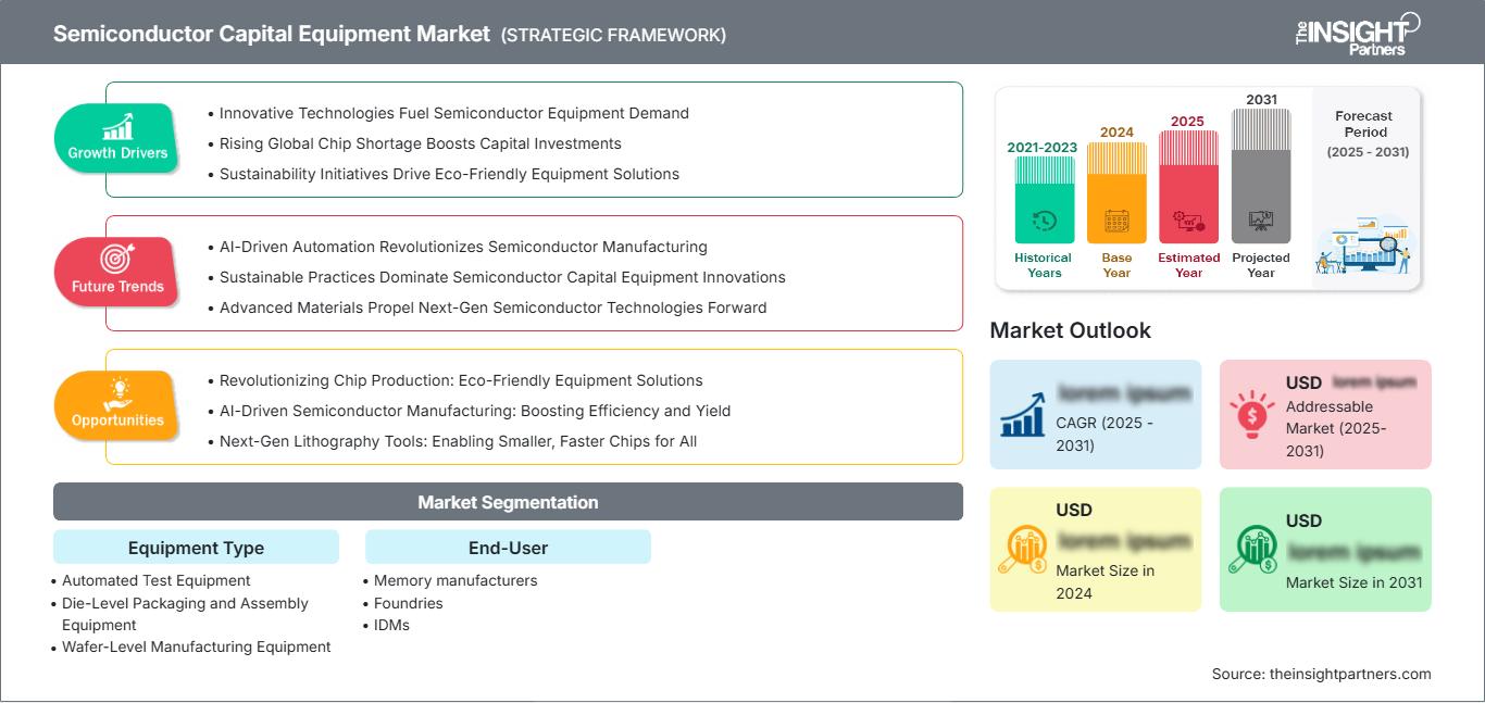
Semiconductor Capital Equipment Market: Strategic Insights
Regional Insights
North America Semiconductor Capital Equipment
North America accounted for an estimated 9–11% Semiconductor Capital Equipment share in 2025 and is expected to grow at a 7.8–8.6% CAGR through 2034. The region is driven by US fab incentives, advanced packaging pilots, and investments in logic, memory, analog, and compound semiconductor capacity. Tool demand is strongest where customers need process transfer, yield stabilization, and domestic supply-chain resilience.
Support for structural growth comes from the US CHIPS Act funding policy, semiconductor workforce training initiatives, and increased demand for data center silicon. Nevertheless, delays in building projects and the qualification of new equipment dampen near-term spending. While growth in Semiconductor Capital Equipment in the region is not as volume-oriented as Asia Pacific, more valuable equipment sets add to its significance.
U.S. Semiconductor Capital Equipment Market
The US represented 82–86% of North America demand in 2025 and is projected to post an 8.0–8.8% CAGR from 2026 to 2034. Domestic capacity additions across Arizona, Texas, Ohio, Idaho, and New York support demand for wafer processing, metrology, packaging, and automated test equipment. Applications are concentrated in AI processors, memory, power management, automotive chips, and defense-grade electronics.
Company presence is reinforced by Applied Materials, Inc., Lam Research Corporation, KLA Corporation, Teradyne, Inc., and ASML Holding N.V. service operations. The US market is notable for higher spending on process control, fab automation, and service contracts because new fabs require rapid yield learning. Semiconductor Capital Equipment trends also point toward advanced packaging clusters linked to HBM, chiplets, and accelerator architectures.
Europe Semiconductor Capital Equipment Market
In Europe, the market was valued at 3–5% in 2025 and expected to expand at a 6.2–7.0% CAGR. Germany is the leading region with demand driven by the requirements of specialty processes, testing, and packaging in automotive semiconductors, power devices, and industrial electronics. The European Chips Act also boosts regional fabs, pilot lines, and research infrastructure in advanced materials and energy-efficient electronics.
The United Kingdom participates through compound semiconductors, design-related prototyping, and academic-industry research, but not in wafer fab expenditure. The demand includes power electronics, photonic technologies, and advanced packaging services. In France, there is growing interest in FD-SOI, sensors, and electronic systems for defense applications. This provides specific demand for lithography, deposition, and metrology equipment linked to resilient supply chains in Europe.
Italy and Spain participate in the regional Semiconductor Capital Equipment market through industrial electronics, automotive supply chains, and a semiconductor R&D ecosystem. This expenditure is lower compared to Germany, yet important for packaging, testing, and specialty manufacturing. Europe’s prospects are dependent on the execution of subsidies, stable energy costs, and customer commitments of automotive, industrial automation, aerospace, and renewable-energy electronics customers.
APAC Semiconductor Capital Equipment Market
APAC accounted for 78–82% share in 2025 and is projected to grow at a 9.7–10.5% CAGR. China remains the largest equipment destination, supported by mature-node localization and selective advanced capacity.
Taiwan and South Korea drive leading-edge foundry, DRAM, NAND, and HBM tool purchases. Japan contributes through materials, lithography, and domestic fab programs, while India is scaling assembly, test, and early wafer-fab ambitions.
Australia remains smaller but relevant for research and compound semiconductor niches. Industrial policy, export-control adaptation, and local supplier ecosystems will define the region’s Semiconductor Capital Equipment Market resilience.
Middle East & Africa Semiconductor Capital Equipment Market
The Middle East & Africa market is expected to expand at a 5.4–6.2% CAGR, led by the UAE’s technology diversification agenda and Saudi Arabia’s industrial investment programs. Demand remains early-stage and focused on packaging, test, R&D, and specialty electronics.
Energy transition, data-center expansion, and sovereign digital infrastructure create long-term semiconductor demand. South Africa contributes through electronics manufacturing, mining technology, and research capacity, but large-scale wafer fab spending remains limited.
Rest of MEA adoption will depend on skilled labor, water availability, power reliability, and anchor customers. The region’s role is more likely to begin with back-end capacity before front-end fabs.
Segmentation Analysis
Equipment Type
Equipment Type is expected to grow at an 8.8–9.6% CAGR from 2026 to 2034. Adoption is shaped by higher process complexity, advanced packaging needs, and increased test intensity. Wafer-level tools dominate spending, while assembly and test equipment gain strategic relevance as chiplet architectures and HBM increase manufacturing steps after wafer fabrication.
- Automated Test Equipment supports higher test coverage for AI processors, HBM, automotive semiconductors, and power devices, making it essential for quality assurance, binning accuracy, and device reliability.
- Die-Level Packaging and Assembly Equipment is gaining strategic importance as chiplets, hybrid bonding, fan-out, and 2.5D packaging raise demand for precise placement, interconnect density, and thermal management.
- Wafer-Level Manufacturing Equipment remains the largest spending category because lithography, deposition, etch, cleaning, ion implantation, and metrology determine yield, throughput, and node migration economics.
End-User
End-User demand is projected to grow at a 9.1–9.9% CAGR during 2026–2034. Foundries remain capital-intensive because they must support advanced logic and mature-node customers simultaneously. Memory manufacturers are accelerating HBM and DRAM equipment purchases, while IDMs invest selectively in power, analog, automotive, and specialty semiconductor lines.
- Memory manufacturers require equipment for DRAM, NAND, and HBM transitions, with demand linked to deposition, etch, inspection, and packaging tools supporting higher layer counts and bandwidth.
- Foundries represent the most diverse customer base, buying tools for leading-edge logic, specialty nodes, and mature processes serving AI, mobile, automotive, connectivity, and industrial applications.
- IDMs prioritize equipment that supports differentiated process platforms, secure supply, and long product lifecycles, especially in power management, sensors, analog chips, and automotive-grade semiconductors.
Opportunity Snapshot
| Segment Name | Revenue Contribution | Trend Tag | Adoption Stage |
| Memory manufacturers | High | HBM Scaling | Scaling |
| Foundries | High | GAA Nodes | Mature |
| IDMs | Medium | Power Chips | Scaling |
Semiconductor Capital Equipment Market Growth Drivers and Impact Analysis
AI and HBM Capacity Expansion
The increasing use of accelerators, high-bandwidth memory, and interconnects in AI infrastructure drives up the equipment intensity of wafer manufacturing, packaging, and test operations. High Bandwidth Memory requires more complex processing than DRAM, whereas the AI chip involves stringent overlay requirements, defect inspection, and thermal packaging control. This trend benefits the Semiconductor Capital Equipment Market because customers' capital expenditure shifts from adding capacity to upgrading capabilities in deposition, etch, metrology, hybrid bonding, and fast test platforms.
Government-Led Manufacturing Localization
Structural demand for semiconductor policy has been driven by the need for assured electronics supply chains on the part of the US, EU, Japan, Korea, China, India, and Middle Eastern economies. On one hand, incentives mitigate risk; on the other, they raise demands for local support services, compliance, training, and redundant suppliers. There is uneven market impact, with high-end fabs affecting high-value front-end equipment, while new ecosystems initially favor assembly, packaging, test, and specialty equipment.
Rising Process Complexity at Advanced Nodes
Advanced nodes require more process steps, tighter tolerances, and increased inspection frequency, thereby making capital equipment a larger share of overall fab spending. Gate-all-around transistors, backside power delivery, multi-patterning, EUV usage, and three-dimensional memory devices drive the need for accurate equipment. The business implications of this are considerable, as buyers now evaluate equipment based on yield contribution, process capability, energy efficiency, and availability, not just price.
Semiconductor Capital Equipment Market Future Trends
Equipment Intelligence and Predictive Fab Control
Future fabs will increasingly rely on technologies such as embedded sensors, digital twins, predictive maintenance, and process control tuning via artificial intelligence to mitigate downtime and increase yield stability. There will be a need for tool suppliers to sell their products together with services such as software and analytics. This will position installed-base knowledge as a key competitive advantage for customers running mixed-node fabs.
Advanced Packaging as a Front-End Adjacent Platform
Advanced packaging will shift from being a back-end activity to an extension of front-end scaling. The advent of chiplets, silicon interposers, hybrid bonding, and fan-out strategies allows engineers to enhance bandwidth and power efficiency by avoiding sole dependence on node reduction. Companies that offer equipment that connects wafer processing, bonding, testing, and thermal management needs will benefit as users create integrated packaging lines for artificial intelligence accelerators, networking devices, and computing machines.
Semiconductor Capital Equipment Market Opportunities
Service-Led Revenue Expansion
Equipment manufacturers could increase their recurring revenue by offering guarantees for uptime, chamber enhancements, process packages, diagnostics, and yield enhancements. With the extended operating lifespans of fabs, together with multiple technology generations, the supplier's ability to provide services becomes an important aspect of purchasing rather than something provided post-purchase. Equipment manufacturers with highly engineered field networks and maintenance platforms could benefit more, especially in locations with new fabs that lack manpower.
Emerging Back-End Manufacturing Hubs
Newcomers to developing semiconductor ecosystems, but without any advanced node manufacturing capacity initially, could start by participating in the assembly, packaging, and testing sector. For example, India, Malaysia, Vietnam, the UAE, and Saudi Arabia are among the countries where policy support, increasing electronics consumption, and manufacturing diversification would generate equipment opportunities. Companies must focus on modular back-end equipment, training, and service collaborations due to scalability.
Recent Developments
- May 2026: Lam Research Corporation reported strong quarterly performance and highlighted demand for etch and deposition systems tied to AI, memory, and advanced packaging applications. The update reinforced the company’s exposure to HBM-related process complexity and continued customer investment in high-performance semiconductor manufacturing capacity.
- April 2026: Worldwide sales of semiconductor manufacturing equipment increased 15% to $135.1 billion in 2025 from $117.1 billion in 2024, driven by continued investment in advanced logic, memory, and AI-related capacity expansion, SEMI, the industry association representing the global electronics design and manufacturing supply chain, reported today. The data is available in the Worldwide Semiconductor Equipment Market Statistics (WWSEMS) report.
- May 2026: India’s semiconductor manufacturing ecosystem continues to expand in 2026, with 13 approved semiconductor projects operational or under development as of May 18, 2026. The latest addition is an ATMP/OSAT facility in Bhiwadi, Rajasthan, inaugurated on May 15, 2026, under the Scheme for Promotion of Manufacturing of Electronic Components and Semiconductors (SPECS). The facility is notable for being the first semiconductor unit established outside the India Semiconductor Mission (ISM).
Frequently Asked Questions

- Comprehensive Market Sizing and Forecast Analysis
- Detailed Segmentation Analysis
- In-Depth Market Dynamics Assessment
- Regional and Country-Level Insights
- Competitive Landscape and Company Benchmarking
- Strategic Business Intelligence
Recent Reports
Testimonials

The Insight Partners' SCADA System Market report is comprehensive, with valuable insights on current trends and future forecasts. The team was highly professional, responsive, and supportive throughout. We are very satisfied and highly recommend their services.
RAN KEDEM Partner, Reali Technologies LTDs
I requested a report on a very specific software market and the team produced the report in a few days. The information was very relevant and well presented. I then requested some changes and additions to the report. The team was again very responsive and I got the final report in less than a week.
JEAN-HERVE JENN Chairman, Future Analytica
We worked with The Insight Partners for an important market study and forecast. They gave us clear insights into opportunities and risks, which helped shape our plans. Their research was easy to use and based on solid data. It helped us make smart, confident decisions. We highly recommend them.
PIYUSH NAGPAL Sr. Vice President, High Beam Global
The Insight Partners delivered insightful, well-structured market research with strong domain expertise. Their team was professional and responsive throughout. The user-friendly website made accessing industry reports seamless. We highly recommend them for reliable, high-quality research services
YUKIHIKO ADACHI CEO, Deep Blue, LLC.
This is the first time I have purchased a market report from The Insight Partners.While I was unsure at first, I visited their web site and felt more comfortable to take the risk and purchase a market report.I am completely satisfied with the quality of the report and customer service. I had several questions and comments with the initial report, but after a couple of dialogs over email with their analyst I believe I have a report that I can use as input to our strategic planning process.Thank you so much for taking the extra time and making this a positive experience.I will definitely recommend your service to others and you will be my first call when we need further market data.
JOHN SUZUKI President and Chief Executive Officer, Board Director, BK Technologies
I wish to appreciate your support and the professionalism you displayed in the course of attending to my request for information regarding to infectious disease IVD market in Nigeria. I appreciate your patience, your guidance, and the fact that you were willing to offer a discount, which eventually made it possible for us to close a deal. I look forward to engaging The Insight Partners in the future, all thanks to the impression you have created in me as a result of this first encounter.
DR CHIJIOKE ONYIA MANAGING DIRECTOR, PineCrest Healthcare Ltd.Reason to Buy
- Informed Decision-Making
- Understanding Market Dynamics
- Competitive Analysis
- Identifying Emerging Markets
- Customer Insights
- Market Forecasts
- Risk Mitigation
- Boosting Operational Efficiency
- Strategic Planning
- Investment Justification
- Tracking Industry Innovations
- Aligning with Regulatory Trends





 Get Free Sample for