
Wafer Foundry Market Growth, Share & Trends by 2034
Coverage: By Type (LiTaO3, Quartz, LiNbO3, Bonded); End User (Consumer Electronics, Automotive, Communications, Others) , and Geography (North America, Europe, Asia Pacific, and South and Central America)
- Status : Data Released
- Report Code : TIPRE00007135
- Category : Electronics and Semiconductor
- No. of Pages : 150
- Available Report Formats :


- Last update date : September 28, 2026


2025 Market Size
US$ 154.92 Bn
Base year value
2034 Forecast
US$ 443.68 Bn
Projected by 2034
CAGR 2026-2034
12.40 %
Growth rate
Addressable Market
US$ 2,616.86 Bn
(2026-2034)
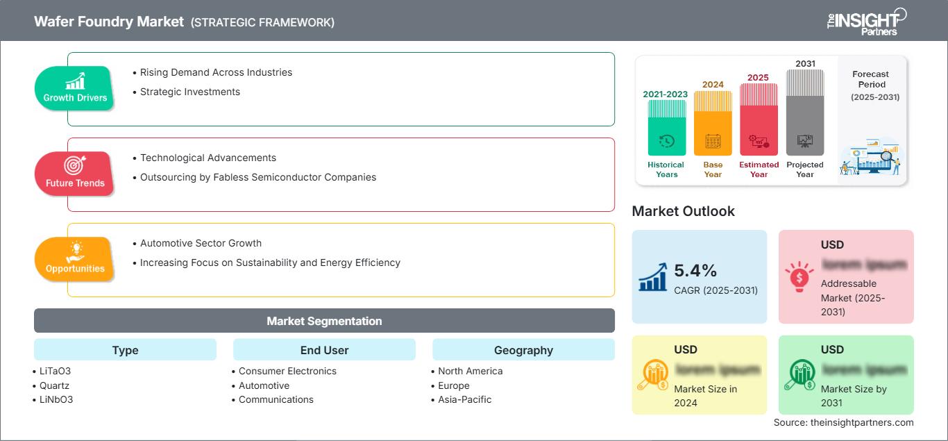
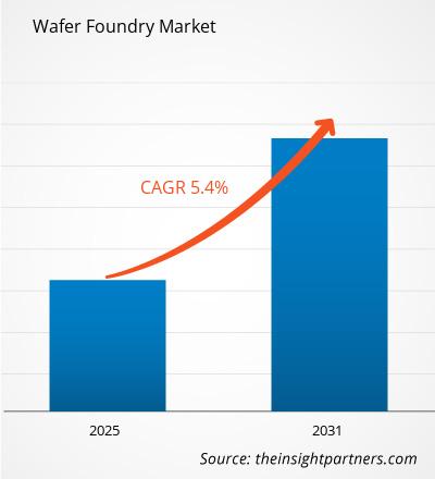
The wafer foundry market is valued at US$ 154.92 Billion in 2025 and is projected to reach US$ 443.68 Billion by 2034, registering a CAGR of 12.40% during 2026–2034. Expansion is being shaped by rising semiconductor content, AI infrastructure, automotive electronics, connectivity upgrades, and continued outsourcing of wafer fabrication to specialized manufacturing partners with scalable process technologies.
North America is expected to record approximately 10–13% CAGR through 2034, supported by semiconductor reshoring, federal incentives, advanced computing investment, and expanding domestic fabrication capacity. The wafer foundry market size in the region is also being influenced by automotive semiconductor localization, cloud infrastructure, aerospace electronics, and strategic supply-chain diversification involving leading foundries and integrated technology companies.
Wafer Foundry Market Assessment and Insights
- North America: The region is estimated to represent 8–10% share in 2025 and grow at a CAGR of 10–13% between 2026–2034, supported by reshoring programs, AI infrastructure, automotive electronics, and new domestic fabrication capacity.
- US: The US represents approximately 70–78% of North America's 2025 demand and is projected to expand at a 10–13% CAGR between 2026–2034, led by advanced computing and supply-chain localization.
- Europe: Europe is estimated at 8–10% share in 2025 and is expected to grow at 8–11% CAGR between 2026–2034, with Germany, France, Italy, Spain, and the UK supporting automotive, industrial, communications, and power semiconductor demand.
- Asia Pacific: Asia Pacific accounts for approximately 74–78% share in 2025 and is projected to expand at 13–16% CAGR between 2026–2034, led by Taiwan, China, South Korea, Japan, and India.
- Largest Segment: Consumer Electronics holds approximately 48–54% market share in 2025 and is projected to expand at a 12–14% CAGR between 2026–2034, reflecting high semiconductor intensity across connected devices.
- High Growth Segment: Automotive is estimated at 14–18% market share in 2025 and is projected to grow at a 15–18% CAGR between 2026–2034, driven by electrification, ADAS, and software-defined vehicles.
- Key companies analyzed in detail: DB HiTek Co., Ltd.; GLOBALFOUNDRIES Inc.; Hua Hong Semiconductor Limited; Powerchip Semiconductor Manufacturing Corporation; Samsung Electronics Co., Ltd.; Semiconductor Manufacturing International Corporation; Taiwan Semiconductor Manufacturing Company Limited; Tower Semiconductor Ltd.; United Microelectronics Corporation; Vanguard International Semiconductor Corporation.
Source: The Insight Partners' analysis based on proprietary research, government publications, company annual reports, investor presentations, industry databases, and expert interviews.
The wafer foundry market has evolved from predominantly cost-focused outsourcing toward differentiated manufacturing ecosystems combining process specialization, advanced packaging, capacity assurance, and geographic diversification. Foundries increasingly balance mature-node utilization with advanced-node investments, while customers seek stable access to wafer capacity for AI accelerators, automotive controllers, connectivity devices, sensors, and power-management components. This shift is strengthening the strategic role of dedicated manufacturing partners.
Looking ahead, the wafer foundry market report indicates that the industry is expected to benefit from capacity expansion outside traditional manufacturing clusters, particularly in the US, Europe, India, Singapore, and other Asian locations. Government incentives, supply-chain resilience programs, and demand visibility from AI infrastructure are supporting long-duration capital commitments. Regulatory emphasis on domestic semiconductor capability is also encouraging customers to qualify multiple manufacturing locations and reduce dependence on single-region production networks.
Wafer Foundry Market Report Scope
| Report Attribute | Details |
|---|---|
| Market size in 2025 | US$ 154.92 Billion |
| Market Size by 2034 | US$ 443.68 Billion |
| Global CAGR (2026 - 2034) | 12.40% |
| Historical Data | 2021-2024 |
| Forecast period | 2026-2034 |
Wafer Foundry Market Analysis
The wafer foundry market growth is closely linked to semiconductor outsourcing, rising chip content per electronic system, and increasing fabrication complexity. The ecosystem consists of IP vendors, EDA companies, wafer suppliers, fabrication equipment vendors, foundries, outsourced assembly and test providers, and original equipment manufacturers. The highest demand will be driven by applications in which the performance, reliability, energy efficiency, and continuous production capability of the semiconductor device impact the economics of the end-product.
A more regional focus is emerging on the supply side. Cutting-edge capacity is still primarily based in East Asia, but capacity expansion is occurring in North America and Europe to increase the security of supply. Mature and specialty processes are strategically relevant due to their importance in automotive, industrial, communication, power management, and consumer applications that have long lifecycles and reliable manufacturing platforms.
The wafer foundry market analysis also highlights an increasingly segmented competitive landscape. Taiwan Semiconductor Manufacturing Company Limited still holds a dominant technological and scale position, whereas Samsung Electronics Co., Ltd., on its part, competes by means of integration in advanced nodes and memory technologies. On their part, GLOBALFOUNDRIES Inc., United Microelectronics Corporation, Semiconductor Manufacturing International Corporation, Tower Semiconductor Ltd., and Vanguard International Semiconductor Corporation offer a specialization and mature-node proposition.
The wafer foundry market forecast indicates that strategic investment is increasingly tied to customer commitments rather than capacity expansion alone. US-based GLOBALFOUNDRIES Inc. is developing US fabrication and packaging facilities, while United Microelectronics Corporation is developing its Singapore operations. Samsung Electronics Co., Ltd. is progressing in the development of its 2nm technology, and Semiconductor Manufacturing International Corporation is raising domestic capacities. DB HiTek Co., Ltd., Hua Hong Semiconductor Limited, Powerchip Semiconductor Manufacturing Corporation, along with others, continue to play an essential role in specific circumstances.
● REPORT CUSTOMIZATION
Tailor This Report To Align With Your Specific Business Requirements
This report can be customized to align precisely with your business objectives, scope, and target markets. Customization options include tailored segmentation, geography, competitive analysis, and strategic insights to support informed decision-making.
Customize This Report →WHAT YOU CAN ADJUST
- ● Segmentations
- ● Geography
- ● Competitive Analysis
- ● Language Preferences
Wafer Foundry Market: Strategic Insights
Regional Insights
North America wafer foundry market
North America is estimated to hold 8–10% of the wafer foundry market share in 2025 and expand at a 10–13% CAGR through 2034. The United States leads the region in terms of demand due to semiconductor localization being an important industry strategy. Artificial intelligence data centers, automobiles, aerospace equipment, communication devices, and industrial automation are some of the applications driving continuous demand for advanced and specialty manufacturing capabilities.
In addition, the region’s supply chain is diversifying geographically. GLOBALFOUNDRIES Inc. is scaling up US manufacturing and advanced packaging, while Taiwan Semiconductor Manufacturing Company Limited continues scaling up Arizona capacity. Commitments by technology, automotive, and communication companies make demand visibility easier in the future. Canada and Mexico participate in the region through their electronics manufacturing ecosystems and supply chain connectivity. However, their wafer fabrication presence is significantly lower than that of the US.
U.S. wafer foundry Market
The U.S. accounts for approximately 70–78% of North America's wafer foundry wafer foundry market share in 2025 and is projected to grow at a 10–13% CAGR through 2034. Domestic investment is being supported by semiconductor incentives, AI infrastructure, automotive localization, defense requirements, and demand for secure supply chains.
Larger firms are widening their application reach into areas like automotive, communication, cloud computing, aerospace, and industrial electronics. GLOBALFOUNDRIES Inc. caters to energy-efficient and connectivity applications, whereas Taiwan Semiconductor Manufacturing Company Limited is ramping up its manufacturing capability. In addition, Samsung Electronics Co., Ltd. has maintained an important manufacturing base in the US as well. The rise in domestically qualified wafers and packages has led customers to opt for regionalized sourcing strategies.
Europe wafer foundry Market
Europe is estimated to represent 8–10% share of the wafer foundry market in 2025 and is expected to expand at an 8–11% CAGR through 2034. Germany retains its status as the dominant regional manufacturing center, which is backed by automotive electronics, industrial automation, power semiconductors, and semiconductor manufacturing clusters. The UK adds value through compound semiconductor, design, photonics, and research competencies, whereas European policies target resilience and strategic manufacturing.
Germany's role is further bolstered by Dresden's manufacturing community, with GLOBALFOUNDRIES Inc.'s expanding manufacturing facilities. France has semiconductor manufacturing and research communities around Grenoble, and Italy is leveraging automotive and power electronics demands. Spain is building semiconductor manufacturing investments and infrastructure. In Europe, automotive electrification, industrial digitalization, renewable energy equipment, and communications infrastructure form a stable demand for specialty and mature manufacturing process technologies along with selected advanced node technologies.
APAC wafer foundry Market
APAC represents approximately 74–78% share in 2025 and is expected to grow at a 13–16% CAGR through 2034. Taiwan continues to lead in manufacturing capacity, followed by China, South Korea, Japan, India, and Australia. Semiconductors continue to have strong ecosystems, supply chains, and engineering resources, along with the backing of their governments.
Domestic manufacturing capacity is growing in China, South Korea is moving ahead in advanced nodes, semiconductor resiliency is being developed in Japan, and an expanded fabricating ecosystem is being built in India. Singapore is growing strategically with new capacity additions. Auto electronics, smartphones, artificial intelligence computing, connectivity, industrial systems, and IoT applications drive the regional demand, as do semiconductor policies for each country.
Middle East & Africa wafer foundry Market
The Middle East and Africa wafer foundry market represents a comparatively small portion of global demand but are projected to expand at approximately 7–10% CAGR through 2034. In Saudi Arabia and UAE, there are investments being made for building a strong technological infrastructure, and South Africa is known to have a strong base in electronics and industries.
There are investments being made in data centers, telecom infrastructure, and smart infrastructure by Saudi Arabia and UAE, and South Africa helps in providing industrial electronics and communications needs. The rest of the region would take time to develop as its energy infrastructure, cloud infrastructure, transportation, and digital connectivity would be developed.
Segmentation Analysis
Type
Wafer foundry market trends indicate that the Type segment is projected to expand at a 10–14% CAGR between 2026–2034. Demand varies according to substrate performance, frequency requirements, thermal characteristics, and application-specific manufacturing specifications. LiTaO3 and LiNbO3 are particularly relevant to high-frequency and communications-oriented applications, while quartz and bonded structures serve specialized performance requirements.
- LiTaO3: LiTaO3 supports high-frequency applications requiring stable electromechanical performance. Its relevance is strengthened by wireless communications, acoustic-wave components, and specialized RF systems where temperature stability and material properties influence device performance.
- Quartz: Quartz remains important for frequency-control and timing applications. Demand is connected with communications equipment, consumer electronics, industrial controls, and automotive electronics requiring stable oscillation and precise timing across operating environments.
- LiNbO3: LiNbO3 is strategically relevant to optical, RF, and acoustic applications because of its strong electro-optic and piezoelectric characteristics. Its adoption benefits from communications infrastructure and increasing requirements for high-speed signal processing.
- Bonded: Bonded wafer structures enable combinations of materials or device layers to achieve application-specific performance. Their strategic importance increases where heterogeneous integration, thermal management, and specialized device architectures require customized substrate configurations.
End User
The End User segment is forecast to grow at a 12–15% CAGR during 2026–2034. Increasing semiconductor content across connected products, vehicles, and communications infrastructure is supporting manufacturing demand. Consumer Electronics remains the largest demand pool, while Automotive is expected to record the fastest expansion as electronic architectures become more complex.
- Consumer Electronics: Consumer electronics generate substantial recurring demand because smartphones, wearables, computing devices, displays, and connected products require increasingly sophisticated semiconductor content. Shorter product cycles also support continuous wafer manufacturing requirements.
- Automotive: Automotive demand is strengthening as electric vehicles, ADAS, infotainment, connectivity, and vehicle-domain controllers increase semiconductor intensity. Long qualification cycles make reliable foundry relationships strategically important for automakers and Tier 1 suppliers.
- Communications: Communications applications require high-performance components for wireless infrastructure, optical networking, RF systems, and connectivity equipment. The transition toward higher data rates and expanded network capacity supports sustained specialized wafer requirements.
- Others: Other end users encompass industrial, healthcare, aerospace, defense, and energy applications where reliability and lifecycle requirements support demand for qualified manufacturing processes and specialized semiconductor architectures.
Opportunity Snapshot
| End User | Revenue Contribution | Trend Tag | Adoption Stage |
| Consumer Electronics | High | Connected Devices | Mature |
| Automotive | High | Vehicle Electrification | Scaling |
| Communications | Medium | 5G Infrastructure | Scaling |
| Others | Medium | Industrial Digitization | Scaling |
Wafer Foundry Market Growth Drivers and Impact Analysis
AI Computing and Data-Center Semiconductor Intensity
AI computing is growing the usage of semiconductors within accelerators, network processors, memory interfaces, power management, and high-bandwidth connectivity devices. This creates a need for higher computational density, driving foundries to invest in their advanced process technology capabilities as well as increase the use of mature technologies employed in the supporting infrastructure. AI compute loads also add increased visibility to wafer capacity planning since hyperscale infrastructure suppliers and silicon vendors often invest significant amounts of time and money before going into production. It makes process qualification, yield management, advanced packaging readiness, and reliable wafer capacity more strategically valuable for foundries. Foundries that can leverage process technology, packaging, and ecosystem readiness can claim a larger share of their customers' programs.
Automotive Electrification and Increasing Electronic Content
Electrification in vehicles will result in increased numbers and variety of semiconductor devices that go into each car. This includes chipsets for energy storage, power conditioning, motor drive, energy charging, thermal regulation, sensing, and communication, as well as processing units and sensor interfaces for ADAS technology. Customers in the automotive industry need products to have prolonged product life cycles, extensive qualification, reliability, and process stability. All of this will favor foundries that can maintain mature node production for a significant amount of time while constantly developing the processes. It is especially valuable in the case of specialty wafer technologies and manufacturing platforms designed for analog, mixed-signal, RF, power, and sensor technologies. With the development of software-defined architectures in vehicles, the dependence of semiconductor demand on car parts will decrease.
Supply-Chain Localization and Government Semiconductor Incentives
Globally, governments are promoting domestic semiconductor fabrication in order to minimize geopolitical risks, transportation delays, and concentration in terms of fabrication capabilities. With the help of incentives, the cost of investment for large fab purchases is being brought down, and the government is encouraging companies to create a regional manufacturing footprint. Such an investment cycle is bringing about change in procurement behavior, where chip designers look into geographic reliability along with yield, process capability, cost, and availability. Therefore, North America and Europe have become important regions for future foundry growth, whereas the APAC region continues to get significant investment due to its manufacturing ecosystem. Localization also helps the ecosystem of other industries such as semiconductor equipment, chemicals, materials, packaging, testing, logistics, and engineering services.
Wafer Foundry Market Future Trends
Distributed Multi-Region Manufacturing Networks
Future strategies for foundries will be geared toward having distributed manufacturing networks rather than being dependent on a single geographic cluster. The customers will tend to qualify several production facilities for critical products, especially when there are applications in areas such as automobiles, communications, aerospace, defense, and infrastructure, where continuous availability of supplies is required. This has led to foundries gearing up with common process platforms across different geographic locations, engineering support for customers, and the ability to manufacture wafer production in conjunction with packaging and testing in that region. Diversifying capacity can make the company capital-intensive; therefore, capacity utilization becomes important. The most successful manufacturing networks will be those that have a combination of standardized process platforms and regionalization rather than trying to replicate all technologies in all facilities.
Heterogeneous Integration and Process-Specialized Manufacturing
Heterogeneous integration is anticipated to impact the strategies of foundries as system designers integrate various technologies, including chiplets, sensors, memory, power devices, and specific accelerators into highly complicated packaging. Such development limits the practice of using the same process technology for all components of the system, which allows customers to choose the most cost-effective or technologically sound technology for each functional block. The transition to such a strategy opens up opportunities for the foundries, which have their own specialty process technologies, advanced packaging collaborations, wafer bonding, and design enablement. It also makes room for smaller fabrication specialists due to the fact that high-value segments might need special technologies in addition to the smallest geometry. Hence, process diversification is likely to remain commercially relevant during the forecast period despite the heavy investments in leading-edge logic.
Wafer Foundry Market Opportunities
Regional Specialty-Fab Platforms
Opportunities are beginning to materialize in regional specialty fab platforms with a focus on applications in automotive, RF, power, industrial, sensors, and communications segments. Such plants will be able to fill strategic gaps without the need for the extremely high capital expenditures needed for the most advanced logic node processes. Opportunities to enhance economics can be found through the securing of anchor customers, matching capacity to qualified demand, and integrating wafer fabrication with either packaging or testing. Europe and North America are areas where such opportunities are particularly relevant, due to the fact that political support and local customer targets will enhance investment cases. Asia-Pacific is an area where such opportunities exist since the growth of domestic electronics ecosystems needs more specialized capacity.
Foundry Partnerships for Automotive and Communications
Strategic partnership with automotive and communications customers represents another avenue of business since both sectors demand consistent manufacturing processes and increasingly complex architectures for semiconductors. It is possible for foundries to create a unique process platform, qualification program, application engineers, and capacity reservations based on the demands of large customers. Such an approach is expected to deliver greater visibility into demand compared to spot capacity availability while providing customers with manufacturing resiliency. The automotive strategic partnerships would be beneficial in power, sensing, connectivity, and control applications, and communications strategy partnerships will be useful in RF, optical, timing, and high-speed interfaces technologies. Firms engaging in such strategic partnerships must focus on process stability, lifecycle management, traceability, cybersecurity, and geographical redundancy.
Frequently Asked Questions

- Comprehensive Market Sizing and Forecast Analysis
- Detailed Segmentation Analysis
- In-Depth Market Dynamics Assessment
- Regional and Country-Level Insights
- Competitive Landscape and Company Benchmarking
- Strategic Business Intelligence
Recent Reports
Testimonials

The Insight Partners provided valuable market intelligence that supported our global go-to-market strategy. Their team was professional, responsive, and attentive to our feedback, providing thoughtful analysis and helpful methodological clarifications throughout the project.
Junmo Kim Chief Financial Officer (CFO), Enertech Co., Ltd.
The Insight Partners' SCADA System Market report is comprehensive, with valuable insights on current trends and future forecasts. The team was highly professional, responsive, and supportive throughout. We are very satisfied and highly recommend their services.
RAN KEDEM Partner, Reali Technologies LTDs
I requested a report on a very specific software market and the team produced the report in a few days. The information was very relevant and well presented. I then requested some changes and additions to the report. The team was again very responsive and I got the final report in less than a week.
JEAN-HERVE JENN Chairman, Future Analytica
We worked with The Insight Partners for an important market study and forecast. They gave us clear insights into opportunities and risks, which helped shape our plans. Their research was easy to use and based on solid data. It helped us make smart, confident decisions. We highly recommend them.
PIYUSH NAGPAL Sr. Vice President, High Beam Global
The Insight Partners delivered insightful, well-structured market research with strong domain expertise. Their team was professional and responsive throughout. The user-friendly website made accessing industry reports seamless. We highly recommend them for reliable, high-quality research services
YUKIHIKO ADACHI CEO, Deep Blue, LLC.
This is the first time I have purchased a market report from The Insight Partners.While I was unsure at first, I visited their web site and felt more comfortable to take the risk and purchase a market report.I am completely satisfied with the quality of the report and customer service. I had several questions and comments with the initial report, but after a couple of dialogs over email with their analyst I believe I have a report that I can use as input to our strategic planning process.Thank you so much for taking the extra time and making this a positive experience.I will definitely recommend your service to others and you will be my first call when we need further market data.
JOHN SUZUKI President and Chief Executive Officer, Board Director, BK Technologies
I wish to appreciate your support and the professionalism you displayed in the course of attending to my request for information regarding to infectious disease IVD market in Nigeria. I appreciate your patience, your guidance, and the fact that you were willing to offer a discount, which eventually made it possible for us to close a deal. I look forward to engaging The Insight Partners in the future, all thanks to the impression you have created in me as a result of this first encounter.
DR CHIJIOKE ONYIA MANAGING DIRECTOR, PineCrest Healthcare Ltd.Reason to Buy
- Informed Decision-Making
- Understanding Market Dynamics
- Competitive Analysis
- Identifying Emerging Markets
- Customer Insights
- Market Forecasts
- Risk Mitigation
- Boosting Operational Efficiency
- Strategic Planning
- Investment Justification
- Tracking Industry Innovations
- Aligning with Regulatory Trends





 Get Free Sample for