
Extreme Ultraviolet Lithography (EUVL) Equipment Market Demand, Trends & Forecast by 2034
Coverage: by Light Source (Laser Produced Plasma, Vacuum Sparks and Gas Discharges); Equipment (Light Source, Mirrors, Masks and Others); and Application (Memory, IDM, Foundry and Others), and Geography (North America, Europe, Asia Pacific, and South and Central America)
- Status : Data Released
- Report Code : TIPTE100000908
- Category : Electronics and Semiconductor
- No. of Pages : 150
- Available Report Formats :


- Last update date : August 10, 2026


2025 Market Size
US$ 10.17 Bn
Base year value
2034 Forecast
US$ 33.4 Bn
Projected by 2034
CAGR 2026-2034
14.12 %
Growth rate
Addressable Market
US$ 187.64 Bn
(2026-2034)
The Extreme Ultraviolet Lithography Equipment Market size is predicted to grow from US$ 10.17 Billion in 2025 to US$ 33.4 Billion in 2034 at a CAGR of 14.12% during the period 2026–2034. It demonstrates the requirement of advanced semiconductor fabrication processes in which EUV systems allow sub-7 nm and future nodes through 13.5 nm patterning of high-density logic, memory, and foundries.
The forecasted CAGR for North America Extreme Ultraviolet Lithography Equipment Market is estimated to grow 11.8-13.0% during 2026–2034 on the back of advanced logic investment, CHIPS Act-related fab capacity expansion, and increasing AI accelerator needs. The U.S. foundry and IDM investment remains focused on migrating towards the latest process technology.
Extreme Ultraviolet Lithography (EUVL) Equipment Market Assessment and Insights
- North America held 12–15% share in 2025 and is growing at a CAGR of 11.8–13.0% during 2026–2034, supported by U.S. advanced-node fabs, AI chip demand, and strategic reshoring policies.
- US represented 86–90% of North American revenue in 2025 and is growing at a CAGR of 12.0–13.2% during 2026–2034, led by Intel, foundry expansion, and AI infrastructure.
- Europe accounted for 6–8% share in 2025 and is growing at a CAGR of 9.8–11.2% during 2026–2034, led by the Netherlands, Germany, Belgium, and France through equipment, optics, and R&D clusters.
- Asia Pacific captured 76–80% share in 2025 and is growing at a CAGR of 14.8–16.0% during 2026–2034, led by Taiwan, South Korea, Japan, and China-linked mature-node equipment demand.
- Largest Segment Light Source held 50–54% market share in 2025 and is growing at a CAGR of 13.6–14.8% during 2026–2034 as laser-produced plasma dominates system cost.
- High Growth Segment Foundry represented 54–58% market share in 2025 and is growing at a CAGR of 15.0–16.2% during 2026–2034, supported by 2 nm and AI accelerator capacity.
- Key companies analyzed in detail: Intel Corporation; Nikon Corporation; SÜSS MicroTec SE; Taiwan Semiconductor Manufacturing Company Limited; Vistec Semiconductor Systems GmbH; Samsung Electronics Co., Ltd.; Veeco Instruments Inc.; ASML Holding N.V.; Canon Inc.; NuFlare Technology, Inc.
Source: The Insight Partners' analysis based on proprietary research, government publications, company annual reports, investor presentations, industry databases, and expert interviews.
EUV lithography technology has developed from being an experimental source power program to become the primary production technology for next-generation wafers. The market uptake has been hastened since foundries demonstrated that EUV would reduce multipatterning, enhance overlay performance, and minimize cycle time for next-generation technology nodes. The Extreme Ultraviolet Lithography Equipment Market involves NA roadmap, optics tolerance, mask defect reduction, and supply chain, in which ASML, ZEISS, TRUMPF, and metrology companies play significant roles in determining the production readiness of EUV technology.
Capital investment will focus on Taiwan, South Korea, the US, Japan, and select European centers of research as AI, HPC, and advanced memory will demand smaller geometries. Export control will influence regional availability, but at the same time will increase capital expenditures on capability, equipment service, and process optimizations. Regulation of semiconductor resilience is likely to secure purchasing visibility even through cyclical wafer-fab equipment spending.
Extreme Ultraviolet Lithography (EUVL) Equipment Market Report Scope
| Report Attribute | Details |
|---|---|
| Market size in 2025 | US$ 10.17 Billion |
| Market Size by 2034 | US$ 33.4 Billion |
| Global CAGR (2026 - 2034) | 14.12% |
| Historical Data | 2021-2024 |
| Forecast period | 2026-2034 |
Extreme Ultraviolet Lithography (EUVL) Equipment Market Analysis
Extreme Ultraviolet Lithography Equipment market drivers include logic, AI accelerators, high-bandwidth memory interfaces, and migration of the foundries to 3 nm, 2 nm, and high-NA nodes. The benefit of using EUV lithography includes simplified patterning as opposed to multiple DUV exposures. ASML reported a total of 535 units of lithography equipment in 2025, reflecting consistent fab investments and installed base growth.
The supply chain involves suppliers of EUV light sources, precision mirrors, masks, stages, vacuum equipment, metrology equipment, photoresists, and wafer fabs. According to the analysis of Extreme Ultraviolet Lithography Equipment Market, the supply dynamics are determined by the power level of the light source, optics yield, up-time, and qualification cycles of the customer. With the price of one EUV scanner going well beyond US$ 180 million, buying decisions will be tied directly to the cost of production.
Competition structure is very consolidated as ASML Holding N.V. is the sole commercial provider of EUV scanners, and Nikon Corporation and Canon Inc. offer products in the DUV, packaging, and alternative lithography segments. Intel Corporation, Taiwan Semiconductor Manufacturing Company Limited, and Samsung Electronics Co., Ltd. drive demand using their advanced-node roadmaps, capacity plans, and NA-high assessment programs.
The investment dynamics are oriented towards high-NA solutions, mask inspection, pellicles, mirror cleaning, and field upgrades that increase productivity without increasing the scanner capacity. The companies supporting neighboring applications for lithography, mask writing, deposition, and process control include SÜSS MicroTec SE, Vistec Semiconductor Systems GmbH, NuFlare Technology, Inc., and Veeco Instruments Inc. Strategic alignment is defined by the ability to address performance issues with uptime, overlay, and defectivity rather than resolution.
● REPORT CUSTOMIZATION
Tailor This Report To Align With Your Specific Business Requirements
This report can be customized to align precisely with your business objectives, scope, and target markets. Customization options include tailored segmentation, geography, competitive analysis, and strategic insights to support informed decision-making.
Customize This Report →WHAT YOU CAN ADJUST
- ● Segmentations
- ● Geography
- ● Competitive Analysis
- ● Language Preferences
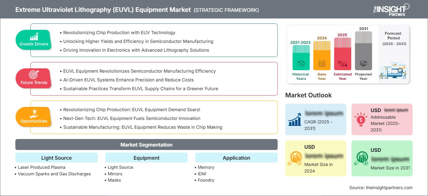
Extreme Ultraviolet Lithography (EUVL) Equipment Market: Strategic Insights
Regional Insights
North America Extreme Ultraviolet Lithography Equipment Market
North America was responsible for 12–15% share of the Extreme Ultraviolet Lithography Equipment Market in 2025 and has been expected to register a CAGR of 11.8–13.0% in 2026–2034. This region depends on investments from the United States in logic and advanced packaging, where EUV usage is linked to AI accelerators, defense electronics, and self-reliant supply chain.
The CHIPS Act, tax advantages, and fabs under construction in Arizona, Ohio, Texas, and New York allow for equipment planning over a decade horizon. Intel Corporation has become the primary domestic customer of EUV, while foundry collaborations and outsourced semiconductor assembly expand demand for related services.
U.S. Extreme Ultraviolet Lithography Equipment Market Market
United States accounted for 86-90% of revenues in North America in 2025, and the country will exhibit a CAGR of 12.0-13.2% during 2026-2034. Demand is driven by process roadmaps of Intel Corporation, advanced foundry capacity build-up, assurance of AI chip availability, and early testing of high NA tools for future nodes.
Application segments favor IDM & foundry over merchant application segments, since economics of EUV is driven by very high wafer counts. Field service of ASML Holding N.V., U.S. suppliers, and customer qualification teams are key factors for uptime. Memory applications are limited in nature, while logic and AI chips dominate capital allocation.
Europe Extreme Ultraviolet Lithography Equipment Market Market
Europe had a 6-8% market share in 2025 and is expected to register growth of 9.8-11.2% CAGR between 2026-2034. The Netherlands dominates due to ASML Holding N.V.'s EUV scanner production monopoly. Germany provides precision optics, lasers, materials and demand for automotive semiconductor chips, while Belgium provides process research via advanced research infrastructure.
UK’s research-oriented market focuses on compound semiconductors, design and specialized equipment services as opposed to volume EUV fab production. France, Italy, and Spain contribute additional demand through their microelectronics, power devices, and packaging programs. Objectives of the European Chips Act enhance funding within the ecosystem, but European scanner demand is smaller compared to Asia due to wafer production being done elsewhere.
APAC Extreme Ultraviolet Lithography Equipment Market Market
The Asia Pacific region was holding 76–80% market share in 2025 and expected to grow with a CAGR of 14.8–16.0% from 2026 to 2034. The Taiwan region is the dominant player through the investments of Taiwan Semiconductor Manufacturing Company Limited. South Korea is next through Samsung Electronics Co., Ltd. memory and foundry segments.
China is limited with EUV restrictions, which drives China towards investments in DUV, packaging, and domestic solutions. India and Australia are smaller, yet policy-driven semiconductor contributors to the region. The region scale is driven by wafer volumes, high customer concentration, closer supply chain, and government support favoring advanced-node security for AI, smartphones, servers, and automotive semiconductors.
Middle East & Africa Extreme Ultraviolet Lithography Equipment Market Market
The growth rate of the Middle East & Africa (MEA) region will be 8.0% to 9.5%, CAGR, during 2026 through 2034. Saudi Arabia and the UAE are considering their own semiconductor ecosystems associated with digital infrastructure and sovereign technology plans, while South Africa will stick with electronics assembly and research, plus select industrial use.
Demand from MEA does not appear likely to include immediate EUV fabs, but energy income diversification, data centers, and national AI initiatives may result in long-term potential in equipment-service, packaging, and design connections. The Rest of MEA will be projects and purchasing dependent upon collaboration and talent development.
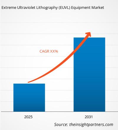
Segmentation Analysis
Light Source
Light Source is projected to grow at a CAGR of 13.6–14.8% during 2026–2034. The Extreme Ultraviolet Lithography Equipment Market scope is shaped by source power, conversion efficiency, collector lifetime, and plasma stability. Light-source improvements directly affect scanner throughput, uptime, and cost per wafer, making this segment the largest value contributor in EUV system architecture.
- Laser Produced Plasma dominates because high-power lasers striking tin droplets generate EUV light suitable for commercial scanners, making performance, debris control, and source uptime decisive purchasing considerations.
- Vacuum Sparks and Gas Discharges remain relevant for research, inspection, and niche generation concepts, but limited power scalability restricts their role in high-volume wafer manufacturing.
Equipment
Equipment is forecast to grow at a CAGR of 13.8–15.0% during 2026–2034. System-level performance depends on integrated light generation, reflective optics, reticles, vacuum stages, and contamination management. Buyers evaluate equipment through throughput, overlay, availability, and lifetime service economics because each scanner must support high-volume wafer production at advanced nodes.
- Light Source equipment carries strategic value because source power and stability determine wafers per hour, tool availability, and the economics of advanced-node production.
- Mirrors are critical because EUV photons require multilayer reflective optics in vacuum, making surface quality, reflectivity, and contamination resistance essential for imaging performance.
- Masks influence yield through defect control, pellicle compatibility, absorber design, and inspection readiness, especially as high-NA EUV tightens patterning margins.
Application
Application is expected to grow at a CAGR of 14.4–15.6% during 2026–2034. Demand is concentrated where EUV reduces layer complexity and supports scaling roadmaps. Memory manufacturers adopt selectively for advanced DRAM and patterning efficiency, IDMs use EUV for internal process leadership, and foundries drive the largest commercial pull through customer diversity.
- Memory adoption is selective but strategically important for DRAM scaling, pattern simplification, and future high-bandwidth memory support linked to AI computing demand.
- IDM users prioritize process control, internal technology leadership, and secure manufacturing capacity, making EUV purchasing dependent on roadmap confidence and fab utilization.
- Foundry applications dominate because leading customers require high-volume advanced logic, AI accelerators, mobile processors, and multi-customer node migration at commercial scale.
Opportunity Snapshot
| Application | Revenue Contribution | Trend Tag | Adoption Stage |
| Memory | Medium | HBM Scaling | Scaling |
| IDM | Medium | Node Control | Mature |
| Foundry | High | AI Nodes | Scaling |
Extreme Ultraviolet Lithography (EUVL) Equipment Market Growth Drivers and Impact Analysis
Advanced AI Chip Demand Raises EUV Tool Intensity
AI Accelerator Chips Need Dense Logic Design, Fast Connectors, and Energy Efficient Process Nodes, Thus Leading to Increased EUV Layers Per Wafer. With More Investment Coming in Hyperscale Data Centers, Chipmakers Are Pushing the Foundries to Adopt Smaller Geometries and Higher Performance-Watts Specifications. There is thus a direct market impact since the fab companies need to procure scanners, services, and process modules at an earlier stage of the technology development life cycle. Suppliers get the benefit of seeing their backlogs while the customers have to incur more capital expenditure and longer qualification periods.
High-NA Transition Resets Advanced Node Economics
The high-NA EUV brings along a change in the numerical aperture that increases the resolution capabilities of sub-2 nm process development, but it alters fab layout considerations, masking considerations, resist considerations, and metrology approaches. The effect goes beyond acquisition of the new scanner; it influences investments in optics, masks, inspection, computational lithography, and process control within the ecosystem. Early adopters have an edge over late learners, whereas conservative users can extend the life of traditional EUV by using multi-patterning and field enhancements. The business impact is that of a phased adoption process.
Semiconductor Sovereignty Supports Long-Cycle Fab Investment
Governments are treating advanced semiconductors as strategic infrastructure, creating incentives for domestic fabrication, talent development, and secure supply chains. This policy environment supports multi-year fab projects even when semiconductor demand cycles soften. For EUV equipment, the impact is stronger geographic diversification of customer sites, higher demand for local service capability, and increased scrutiny of export compliance. However, sovereignty programs cannot instantly create EUV ecosystems because optics, source technology, masks, and process know-how remain highly specialized. Market participants with proven field support and regulatory discipline gain preference in strategic fab programs.
Extreme Ultraviolet Lithography (EUVL) Equipment Market Future Trends
AI-Assisted Lithography Control Moves Into Production
Extreme Ultraviolet Lithography Equipment Market trends point toward AI-assisted process control becoming embedded in scanner optimization, overlay correction, defect prediction, and preventive maintenance. Future fabs will use larger equipment data sets to predict source instability, optics contamination, stage drift, and resist interactions before yield losses appear. This trend will favor suppliers able to combine hardware expertise with software, computational lithography, and secure data integration. Customers will evaluate tools not only by resolution and throughput, but also by how quickly software can improve availability and reduce wafer excursions.
Mask and Pellicle Innovation Becomes a Yield Differentiator
As EUV moves into denser logic and high-NA exposure, mask quality and pellicle performance will become more important to yield economics. Future reticles must manage absorber shadowing, defect inspection, thermal load, and contamination without compromising imaging. This will increase investment in mask writers, actinic inspection, repair tools, and materials engineering. The trend also changes customer qualification behavior because a scanner cannot deliver its full value unless the mask ecosystem is production-ready. Suppliers that reduce defect escape and improve pellicle durability will gain strategic relevance.
Extreme Ultraviolet Lithography (EUVL) Equipment Market Opportunities
High-NA Ecosystem Readiness Services
Extreme Ultraviolet Lithography Equipment Market Forecasts support investment in readiness services around high-NA tool installation, fab layout adaptation, mask qualification, resist screening, and metrology correlation. Customers will need help translating early research exposure results into manufacturable processes. Equipment-adjacent firms can build revenue by offering calibration, contamination control, computational lithography support, and field-service training. This opportunity is attractive because high-NA adoption requires coordinated ecosystem changes rather than a single tool purchase. Suppliers that reduce ramp risk can participate before full high-volume production begins.
Installed-Base Productivity Upgrades
Installed-base upgrades represent a practical opportunity because fabs seek higher wafers per hour, better overlay, and lower downtime from tools already in production. Field upgrades, source improvements, software releases, and maintenance analytics can improve economics without waiting for new scanner delivery. This opportunity benefits ASML Holding N.V. and specialist suppliers involved in optics, masks, metrology, and subsystems. Customers also value upgrades because they protect capital productivity during demand swings. The installed base becomes a recurring revenue platform linked to uptime, yield, and process-node extension.
Recent Developments
- July 2026: ASML Holding N.V. (ASML) reported that Intel Foundry is using ASML’s High NA EUV technology on the Intel 18A process node to produce a subset of its Intel Core Ultra Series 3 processors. This milestone marks an important step in demonstrating High NA EUV readiness in a production environment. ASML and Intel have worked closely for decades to advance lithography technology and support the continued scaling of semiconductors. The high numerical aperture extreme ultraviolet (High NA EUV) lithography process is an important next step in EUV lithography, developed by ASML to enable more precise patterning for advanced chip manufacturing.
- February 2026: Qnity Electronics, Inc. (“Qnity”) (NYSE: Q), a premier technology solutions leader across the semiconductor value chain, announced the expansion of its offerings for extreme ultraviolet (EUV) lithography with the introduction of the Eon™ EUV photoresist product family. The addition strengthens Qnity’s commitment to delivering next-generation solutions that power the next leap in advanced node semiconductor manufacturing.
- September 2025: SK hynix Inc. (or “the company”, www.skhynix.com) announced that it has assembled the industry’s first High NA* EUV* lithography system for mass production at the M16 fabrication plant in Icheon, South Korea.
Frequently Asked Questions

- Comprehensive Market Sizing and Forecast Analysis
- Detailed Segmentation Analysis
- In-Depth Market Dynamics Assessment
- Regional and Country-Level Insights
- Competitive Landscape and Company Benchmarking
- Strategic Business Intelligence
Recent Reports
Testimonials

The Insight Partners' SCADA System Market report is comprehensive, with valuable insights on current trends and future forecasts. The team was highly professional, responsive, and supportive throughout. We are very satisfied and highly recommend their services.
RAN KEDEM Partner, Reali Technologies LTDs
I requested a report on a very specific software market and the team produced the report in a few days. The information was very relevant and well presented. I then requested some changes and additions to the report. The team was again very responsive and I got the final report in less than a week.
JEAN-HERVE JENN Chairman, Future Analytica
We worked with The Insight Partners for an important market study and forecast. They gave us clear insights into opportunities and risks, which helped shape our plans. Their research was easy to use and based on solid data. It helped us make smart, confident decisions. We highly recommend them.
PIYUSH NAGPAL Sr. Vice President, High Beam Global
The Insight Partners delivered insightful, well-structured market research with strong domain expertise. Their team was professional and responsive throughout. The user-friendly website made accessing industry reports seamless. We highly recommend them for reliable, high-quality research services
YUKIHIKO ADACHI CEO, Deep Blue, LLC.
This is the first time I have purchased a market report from The Insight Partners.While I was unsure at first, I visited their web site and felt more comfortable to take the risk and purchase a market report.I am completely satisfied with the quality of the report and customer service. I had several questions and comments with the initial report, but after a couple of dialogs over email with their analyst I believe I have a report that I can use as input to our strategic planning process.Thank you so much for taking the extra time and making this a positive experience.I will definitely recommend your service to others and you will be my first call when we need further market data.
JOHN SUZUKI President and Chief Executive Officer, Board Director, BK Technologies
I wish to appreciate your support and the professionalism you displayed in the course of attending to my request for information regarding to infectious disease IVD market in Nigeria. I appreciate your patience, your guidance, and the fact that you were willing to offer a discount, which eventually made it possible for us to close a deal. I look forward to engaging The Insight Partners in the future, all thanks to the impression you have created in me as a result of this first encounter.
DR CHIJIOKE ONYIA MANAGING DIRECTOR, PineCrest Healthcare Ltd.Reason to Buy
- Informed Decision-Making
- Understanding Market Dynamics
- Competitive Analysis
- Identifying Emerging Markets
- Customer Insights
- Market Forecasts
- Risk Mitigation
- Boosting Operational Efficiency
- Strategic Planning
- Investment Justification
- Tracking Industry Innovations
- Aligning with Regulatory Trends





 Get Free Sample for