
Non-Conductive Ink Market Growth, Share & Trends by 2034
Coverage: by Substrate (Glass, Ceramic, Acrylic); Application (PCB Panels, Pv Panels, Led Packaging, Others) , and Geography (North America, Europe, Asia Pacific, and South and Central America)
- Status : Data Released
- Report Code : TIPRE00008579
- Category : Chemicals and Materials
- No. of Pages : 150
- Available Report Formats :


- Last update date : September 15, 2026


2025 Market Size
US$ 204.99 Mn
Base year value
2034 Forecast
US$ 525.59 Mn
Projected by 2034
CAGR 2026-2034
11.03 %
Growth rate
Addressable Market
US$ 3,227.81 Mn
(2026-2034)
The non-conductive ink market size is expanding as printed electronics, photovoltaic devices, LED packaging, and multilayer circuit architectures increasingly require electrically insulating functional layers. The market was valued at US$ 204.99 Million in 2025 and is projected to reach US$ 525.59 Million by 2034, registering a CAGR of 11.03% during 2026–2034. Growth is supported by demand for dielectric insulation, surface protection, interlayer separation, and reliable printing on rigid and emerging flexible substrates.
North America remains an important technology and application center, with an estimated 8.5–10.0% CAGR during 2026–2034. Semiconductor packaging development, printed circuit innovation, and investment in advanced electronics manufacturing are supporting adoption. The region also benefits from established material suppliers, specialized ink formulators, and research ecosystems connecting ink chemistry with printed and flexible electronic production.
Non-Conductive Ink Market Assessment and Insights
- North America accounts for a 22–26% non-conductive ink Market share in 2025 and is expected to grow at a 8.5–10.0% CAGR between 2026–2034. Demand is supported by printed electronics R&D, semiconductor packaging, automotive electronics, and domestic electronics manufacturing investments.
- US represents approximately 72–78% of North America's share in 2025, expanding at a 8.8–10.2% CAGR during 2026–2034. Printed electronics, advanced packaging, and flexible circuitry remain key demand areas.
- Europe holds a 25–29% share in 2025 and is projected to register a 9.0–10.5% CAGR between 2026–2034, led by Germany, France, the UK, Italy, and the Netherlands through automotive electronics and industrial printing applications.
- Asia Pacific represents a 39–43% share in 2025 and is anticipated to grow at a 12.0–13.5% CAGR during 2026–2034. China, Japan, South Korea, and India benefit from electronics manufacturing, photovoltaic production, and semiconductor investment.
- Largest Segment: Printed Circuit Boards account for a 45–50% market share in 2025, growing at a 10.0–11.5% CAGR during 2026–2034, supported by multilayer insulation and circuit protection.
- High Growth Segment: Photovoltaic Panel applications hold a 15–20% market share in 2025, expanding at a 13.0–15.0% CAGR during 2026–2034, supported by advanced cell architectures and printed functional layers.
- Key companies analyzed in detail: Applied Cavitation Inc., Applied Ink Solutions, Dow Inc., Henkel AG & Co. KGaA, Nagase & Co., Ltd., NovaCentrix, Poly-Ink, Snab Graphix India Private Limited, Sun Chemical Corporation, and Teikoku Printing Inks Mfg. Co., Ltd.
Source: The Insight Partners' analysis based on proprietary research, government publications, company annual reports, investor presentations, industry databases, and expert interviews.
In terms of the production technologies, the trend will shift away from traditional screen-printing inks towards dielectric and insulator materials that can be used in combination with inkjet printing, direct write, multilayer printing, and high-resolution printing. Formulators need to consider balancing their products between electrical resistance and adhesion properties, curing speed, dimension stability, heat-resistance, and compatibility with conductive inks.
The future non-conductive ink Market growth will occur primarily in the Asia-Pacific region due to growth in capacity in electronics, solar, and semiconductor industries. The development in Europe will be driven by automobile electrification and material efficiency needs, whereas growth in North America will be driven by semiconductor and advanced packaging industry. In terms of formulators, they need to focus on low curing temperatures, low solvent level, recyclability, and substrate compatibility.
Non-Conductive Ink Market Report Scope
| Report Attribute | Details |
|---|---|
| Market size in 2025 | US$ 204.99 Million |
| Market Size by 2034 | US$ 525.59 Million |
| Global CAGR (2026 - 2034) | 11.03% |
| Historical Data | 2021-2024 |
| Forecast period | 2026-2034 |
Non-Conductive Ink Market Analysis
The non-conductive ink market is highly correlated with the adoption of multilayer printed electronics, where insulating layers ensure that conductive traces do not experience electrical shorts. The value chain starts from polymeric binders, resins, solvents, dielectrics, pigments, and other ingredients, and continues through formulation, dispersion, quality control, packaging, and end-use qualification. Ink providers need to increasingly reconcile their formulation properties with printing machines and substrates.
According to the non-conductive ink Market report, yield rates have become an additional demand driver instead of just the quantity of prints. For example, insufficient adhesion, poor curing, cracks formation or layer incompatibility can result in rejects in PCB, LED, photovoltaic and sensors applications. As a result, buyers more often than not assess such parameters as dielectric strength, surface resistance, viscosity, curing pattern, resolution and processing compatibility.
The non-conductive ink market forecast shows that the competitive landscape is highly fragmented and comprises diverse chemical manufacturers, specialized ink developers, and experts in printed electronics. Henkel and Sun Chemical have a wide range of functional material portfolio, while NovaCentrix focuses on advanced printed electronics materials and photonics. Teikoku Printing Inks and Applied Ink Solutions cater to the specific needs for printing applications, whereas Nagase has presence in both specialty materials and electronics value chains.
Investments in the non-conductive ink Market are made in customized formulation, digital deposition capability, and improved environmental chemistries. Dow Inc. offers expertise in polymers and materials, while Poly-Ink specializes in functional ink solutions. Snab Graphix India Private Limited provides local manufacturing facilities, and Applied Cavitation Inc. has specialized technology solutions. Competitive advantage will depend on faster qualification, reproducibility in printing, substrate compatibility, and capability to integrate dielectric formulations in multilayer production processes.
● REPORT CUSTOMIZATION
Tailor This Report To Align With Your Specific Business Requirements
This report can be customized to align precisely with your business objectives, scope, and target markets. Customization options include tailored segmentation, geography, competitive analysis, and strategic insights to support informed decision-making.
Customize This Report →WHAT YOU CAN ADJUST
- ● Segmentations
- ● Geography
- ● Competitive Analysis
- ● Language Preferences
Non-Conductive Ink Market: Strategic Insights
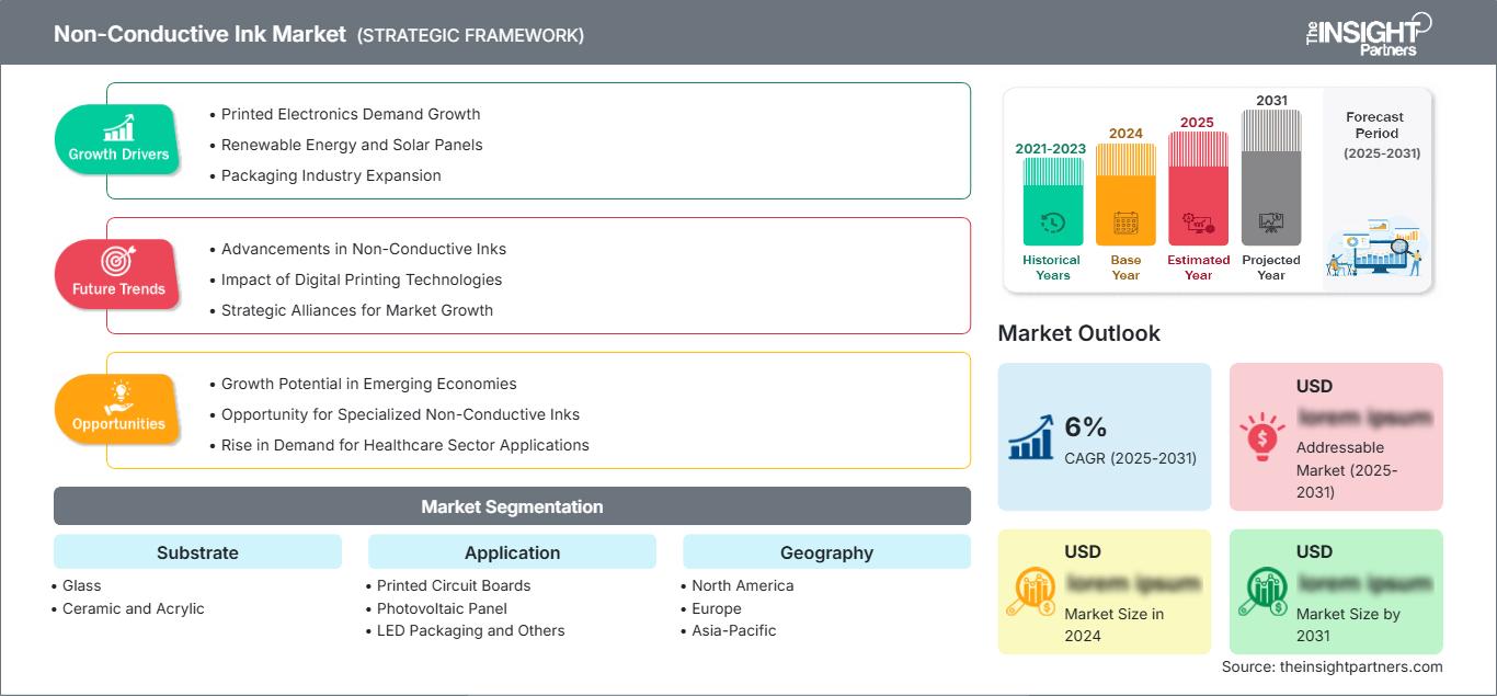
Regional Insights
North America non-conductive ink market
North America represents a 22–26% share in 2025 and is projected to grow at an 8.5–10.0% CAGR during 2026–2034. US domination in the region occurs via semiconductor packaging, automotive electronics, printing of sensors, flexible circuits, and advanced electronics research. Canada helps out via the development of special materials and electronics manufacturing.
Regional demand is fueled by reshoring trends, investments in semiconductors, and additive manufacturing of electronic devices. Clients need dielectric materials that cure at lower temperatures and do not lose adhesion during multilayer assembly. Supplier expertise in formulating materials and application engineering is significant since printed electronics often use custom substrates and curing conditions.
U.S. non-conductive ink Market
The US represents approximately 72–78% of North America's share in 2025 and is expected to expand at an 8.8–10.2% CAGR through 2034. There is demand for printed circuit boards, semiconductor packaging, sensors, automotive interface applications, and flexible electronics. There are specialized vendors and technology providers to support local formulating and prototyping efforts.
Application trends are towards lighter and thinner electronic devices. Multilayer printing has increased the need for effective insulation materials between conductive pathways, and advanced packaging applications demand high deposition accuracy and thermal stability. Having such vendors like Dow Inc., NovaCentrix, and Applied Ink Solutions in the region has helped the technology landscape considerably.
Europe non-conductive ink Market
Europe holds a 25–29% share in 2025 and is expected to grow at a 9.0–10.5% CAGR, with Germany remaining the leading country. The United Kingdom sustains demand through research and specialty manufacturing in the field of printed electronics, and Germany enjoys an advantage because of its automotive electronics, automation, and molded electronics.
France is contributing due to the development of aerospace, automotive, and electronics, while Italy is supporting through specialty printing and industrial equipment applications. Spain is gaining importance because of its photovoltaic production and renewable energy technologies. In the region, material efficiency, reduced emissions, and recyclability are now becoming key criteria for formulation.
APAC non-conductive ink Market
APAC accounts for a 39–43% share in 2025 and is projected to register a 12.0–13.5% CAGR. China is the dominant market, with strength in electronics manufacturing and photovoltaics manufacturing. Japan and South Korea are contributing via high-end displays, semiconductors, and automotive electronics; and India and Australia have emerging demand.
The electronics supply chain from China is well developed and large in scale, while the Japan electronics market is focused on precision materials and reliability. South Korea has strong capabilities in displays and semiconductors; and India is developing capacity in electronics manufacturing. Government support for domestic semiconductor and solar manufacturing will enhance demand for functional insulators.
Middle East & Africa non-conductive ink Market
Middle East and Africa represents a smaller but emerging opportunity, with demand concentrated in Saudi Arabia, the UAE, South Africa, and the Rest of MEA. The region is projected to grow at approximately 7.0–9.0% CAGR during 2026–2034, supported by electronics localization, solar projects, and industrial modernization.
Saudi Arabia and the UAE are investing in advanced manufacturing and renewable-energy infrastructure, creating opportunities for photovoltaic-related materials. South Africa remains the principal southern African market for industrial electronics and specialty printing. Adoption is currently constrained by limited local formulation capacity, making imported specialty inks and regional distribution partnerships important to market development.
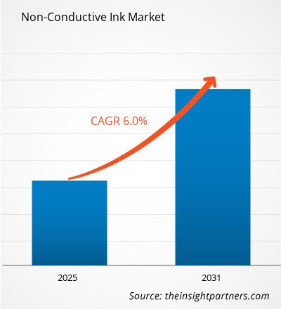
Segmentation Analysis
Substrate
The Substrate segment in the non-conductive ink market is projected to expand at a 10.0–11.5% CAGR during 2026–2034. Demand depends on surface energy, thermal stability, adhesion, dielectric performance, and curing compatibility. Glass remains important for rigid electronics and photovoltaic applications, while ceramic supports high-temperature electronic structures. Acrylic substrates provide opportunities in lightweight displays, automotive interfaces, and specialty printed electronics.
- Glass remains important for photovoltaic panels, LED-related structures, displays, and rigid electronics because of dimensional stability, optical properties, and compatibility with high-resolution functional printing.
- Ceramic supports demanding electronic applications requiring thermal stability, chemical resistance, and electrical insulation. Its strategic importance increases in high-temperature and high-reliability circuit environments.
- Acrylic provides lightweight and design flexibility for display interfaces, automotive components, and decorative electronics, particularly where transparency, thermoformability, and lower component weight influence product architecture.
Application
The Application segment is expected to register a 11.0–12.5% CAGR during 2026–2034. Adoption is being shaped by the growing need for insulation, circuit separation, protection, and controlled dielectric properties in increasingly compact electronic structures. Printed circuit boards remain the largest application, while photovoltaic and LED applications provide additional growth opportunities.
- Printed Circuit Boards represent the leading application because multilayer circuit construction requires reliable insulation between conductive pathways. Material consistency, dielectric strength, curing behavior, and compatibility with established PCB processes remain key purchasing criteria.
- Photovoltaic Panel applications benefit from continued cell efficiency improvements and increasingly sophisticated architectures. Insulating formulations can support electrical isolation and functional layer formation while meeting demanding thermal and outdoor durability requirements.
- LED Packaging uses insulating materials to separate functional elements and protect electronic structures. Growth is associated with compact lighting modules, displays, automotive lighting, and higher-density electronics requiring reliable thermal and electrical performance.
Opportunity Snapshot
| Application | Revenue Contribution | Trend Tag | Adoption Stage |
|---|---|---|---|
| Printed Circuit Boards | High | Multilayer PCBs | Mature |
| Photovoltaic Panel | Medium | Cell Efficiency | Scaling |
| LED Packaging | Medium | MiniLED Packaging | Scaling |
| Others | Low | Sensor Integration | Emerging |
Non-Conductive Ink Market Growth Drivers and Impact Analysis
Expansion of multilayer and flexible printed electronics
Printed electronics manufacturers are increasing the number of functional layers incorporated into compact devices, creating a direct requirement for electrically insulating materials between conductive structures. The use of non-conducting inks allows for circuit crossings, dielectric separation, insulation, and controlled layer spacing without needing conventional etching and lamination procedures on every construction. Flexible electronics become another factor that raises the demands on inks since the latter need to be capable of tolerating bending, stretching, heating, and mechanical deformations. It may result not only in an increase in the volume of materials used but also in higher certification standards. Those ink producers which have proven the reliability of their products through deposition on flexible polymers, glass, and ceramics will be able to win high-value orders.
Increasing photovoltaic manufacturing and cell architecture complexity
Photovoltaic manufacturing is becoming increasingly dependent on advanced cell architectures, finer printed features, and improved electrical isolation. As companies continue their drive towards increased efficiency and resource use in their operations, insulating films may be applied in order to isolate electrical pathways as well as in order to construct increasingly complex devices. The growth of capacity for solar manufacturing in China, India, Southeast Asia, Europe, and the Middle East means that there will be more channels through which there will be demand for functional printables. As such, formulations should be able to stand up to exposure outdoors, temperature changes, and long periods of operation, thus durability becomes an important purchasing factor. The impact on suppliers is dual in nature – volume increases as well as technical demands.
Growth of integrated electronic surfaces and automotive interfaces
Automotive interiors are moving toward integrated displays, touch controls, illuminated surfaces, sensors, and electronically functional decorative components. These architectures often require conductive and non-conductive layers to coexist within thin molded or thermoformed structures. The insulating inks have the potential of being used for creating separation between the electrical connections while keeping the visual integrity and allowing for multilayer printing. It is important for the development since interfaces inside the cabin of electric cars include sensors, lighting, heating, and connectivity and the components are tightly fitted in a limited space. Therefore, qualification criteria become heat, humidity, chemical, forming, and molding resistance. It is an opportunity for ink suppliers to create special formulas rather than just commodity products.
Non-Conductive Ink Market Future Trends
Low-temperature and energy-efficient curing
The non-conductive ink Market trends show that formulations of the future are going to rely heavily on low-temperature and fast cure systems. This is due to the fact that formulators are likely to use thermally sensitive polymer film substrates and multi-layer structures which might deform and degrade at normal temperature cure levels. The use of UV cure, dual cure and energy efficient chemistry can help to lower the amount of heat used and at the same time increase the production volume. The formulators may also try to perfect their curing window so that the insulation materials do not damage the printed conductive material. In a digital environment where line speed and cure efficiency are important to production cost, this is critical. Those who can maintain good dielectric properties while lowering energy input have an advantage.
Higher-resolution dielectric printing for compact electronics
Miniaturization will encourage development of insulating inks capable of producing thinner, more uniform, and more precisely registered layers. As conductive traces become narrower and component density rises, dielectric materials must maintain electrical isolation without creating excessive layer thickness. Inkjet and direct-write systems can enable localized deposition, reducing material consumption and supporting complex multilayer structures. Formulations will increasingly be evaluated for droplet behavior, surface interaction, drying profile, edge definition, and dimensional stability. This trend can broaden the addressable application base toward fine-pitch electronics, wearable devices, advanced sensors, and integrated molded electronics. Suppliers that combine high print resolution with robust dielectric properties may increasingly participate in applications previously dependent on conventional photolithography, lamination, or mechanically patterned insulating films.
Non-Conductive Ink Market Opportunities
Localized formulation and application-development centers in Asia
Asia Pacific offers opportunities for suppliers to establish localized technical centers near major electronics, photovoltaic, display, and semiconductor clusters. Local application laboratories can shorten qualification cycles by allowing customers to test formulations against regional substrates, printing equipment, and curing systems. China, Japan, South Korea, India, and Southeast Asia each present different manufacturing requirements, making standardized global formulations less effective for every application. Technical centers can support customization without requiring complete production relocation. Suppliers can also develop partnerships with electronics manufacturers, universities, equipment providers, and material distributors. Such ecosystems can create recurring demand through co-development and qualification programs. The strongest opportunity is likely to come from combining local technical support with centralized formulation expertise and scalable manufacturing capacity.
Specialized dielectric solutions for advanced packaging and photovoltaics
Advanced packaging and photovoltaic manufacturing provide opportunities for premium formulations designed around specific process requirements rather than general-purpose insulation. Semiconductor packaging requires controlled thickness, thermal stability, dimensional precision, and reliable interlayer performance, while photovoltaic applications emphasize outdoor durability, electrical isolation, and process compatibility. Suppliers can pursue higher-value opportunities by developing application-specific grades validated alongside customer manufacturing processes. Partnerships with printing-equipment manufacturers can further improve deposition reliability and reduce qualification barriers. Product portfolios can also be structured around curing temperature, deposition method, substrate chemistry, and dielectric requirements. Such specialization may reduce direct price competition and create stronger customer retention because changing an approved functional ink can require substantial process requalification and reliability testing.
Recent Developments
- April 8, 2025: Saralon GmbH introduced new ink sets for stretchable membrane switches, heaters, and electroluminescent displays. The company states that its dielectric inks are designed for applications including electroluminescent displays.
- 2025: Pröll GmbH introduced NORIPHAN HTR N 990/011 NC, a carbon-black-free non-conductive black ink for IMD/FIM printed electronics. The formulation provides high electrical resistance and radar transmissibility while targeting thermal resistance, hydrolysis resistance, and adhesion requirements relevant to automotive applications.
Frequently Asked Questions

- Comprehensive Market Sizing and Forecast Analysis
- Detailed Segmentation Analysis
- In-Depth Market Dynamics Assessment
- Regional and Country-Level Insights
- Competitive Landscape and Company Benchmarking
- Strategic Business Intelligence
Recent Reports
Testimonials

The Insight Partners' SCADA System Market report is comprehensive, with valuable insights on current trends and future forecasts. The team was highly professional, responsive, and supportive throughout. We are very satisfied and highly recommend their services.
RAN KEDEM Partner, Reali Technologies LTDs
I requested a report on a very specific software market and the team produced the report in a few days. The information was very relevant and well presented. I then requested some changes and additions to the report. The team was again very responsive and I got the final report in less than a week.
JEAN-HERVE JENN Chairman, Future Analytica
We worked with The Insight Partners for an important market study and forecast. They gave us clear insights into opportunities and risks, which helped shape our plans. Their research was easy to use and based on solid data. It helped us make smart, confident decisions. We highly recommend them.
PIYUSH NAGPAL Sr. Vice President, High Beam Global
The Insight Partners delivered insightful, well-structured market research with strong domain expertise. Their team was professional and responsive throughout. The user-friendly website made accessing industry reports seamless. We highly recommend them for reliable, high-quality research services
YUKIHIKO ADACHI CEO, Deep Blue, LLC.
This is the first time I have purchased a market report from The Insight Partners.While I was unsure at first, I visited their web site and felt more comfortable to take the risk and purchase a market report.I am completely satisfied with the quality of the report and customer service. I had several questions and comments with the initial report, but after a couple of dialogs over email with their analyst I believe I have a report that I can use as input to our strategic planning process.Thank you so much for taking the extra time and making this a positive experience.I will definitely recommend your service to others and you will be my first call when we need further market data.
JOHN SUZUKI President and Chief Executive Officer, Board Director, BK Technologies
I wish to appreciate your support and the professionalism you displayed in the course of attending to my request for information regarding to infectious disease IVD market in Nigeria. I appreciate your patience, your guidance, and the fact that you were willing to offer a discount, which eventually made it possible for us to close a deal. I look forward to engaging The Insight Partners in the future, all thanks to the impression you have created in me as a result of this first encounter.
DR CHIJIOKE ONYIA MANAGING DIRECTOR, PineCrest Healthcare Ltd.Reason to Buy
- Informed Decision-Making
- Understanding Market Dynamics
- Competitive Analysis
- Identifying Emerging Markets
- Customer Insights
- Market Forecasts
- Risk Mitigation
- Boosting Operational Efficiency
- Strategic Planning
- Investment Justification
- Tracking Industry Innovations
- Aligning with Regulatory Trends





 Get Free Sample for