
2D Electronics Market Trends, Demand & Growth by 2034
2D Electronics Market Size and Forecasts (2021–2034), Global and Regional Share, Trends, and Growth Opportunity Analysis by Product Type (Optoelectronic Devices and Electronic Devices); Application (Biomolecular Sensing, Electro Mechanical Systems, Electronics Devices, Energy and Harvesting Devices, Medical Application, Optical Communications, Security Display and Imaging, Solar Cells Batteries, and Flexible Electronics); and Geography
- Status : Data Released
- Report Code : TIPRE00026898
- Category : Electronics and Semiconductor
- No. of Pages : 150
- Available Report Formats :


- Last update date : July 13, 2026


2025 Market Size
US$ 15.8 Bn
Base year value
2034 Forecast
US$ 31.75 Bn
Projected by 2034
CAGR 2026-2034
9.12 %
Growth rate
Addressable Market
US$ 225.63 Bn
(2026-2034)
The 2D Electronics Market is valued at US$ 15.8 billion in 2025 and is projected to reach US$ 31.75 billion by 2034, advancing at a CAGR of 9.12% from 2026 to 2034. The market is moving toward application-specific commercialization as atomically thin materials support flexible circuits, optoelectronic devices, high-sensitivity sensors, energy harvesting structures, and advanced medical electronics across semiconductor and specialty device ecosystems.
North America is expected to expand at an estimated CAGR of 8.4%–9.0%, supported by advanced semiconductor research, defense-linked sensing demand, and medical device innovation. The region benefits from university-industry collaboration, nanofabrication infrastructure, and rising demand for compact, low-power electronics. Investment in photonics, flexible diagnostics, and secure imaging platforms is strengthening regional commercialization prospects for the 2D Electronics Market.
2D Electronics Market Assessment and Insights
- North America: Share in 2025 is estimated at 24%–28%, with CAGR between 2026–2034 of 8.4%–9.0%, driven by photonics, defense sensing, and biomedical device pilots.
- US: Share in 2025 is 78%–82% of North America, with CAGR between 2026–2034 of 8.6%–9.2%, supported by semiconductor design and research commercialization.
- Europe: Share in 2025 is 23%–27%, with CAGR between 2026–2034 of 8.7%–9.3%; Germany leads, while the UK, France, Italy, and Spain support materials and photonics development.
- Asia Pacific: Share in 2025 is 38%–43%, with CAGR between 2026–2034 of 9.4%–10.0%; China leads, followed by Japan, South Korea, India, and Australia.
- Largest Segment: Flexible Electronics held 24%–28% market share in 2025 and is projected to grow at a CAGR of 9.6%–10.2% during 2026–2034.
- High Growth Segment: Biomolecular Sensing held 11%–14% of the 2D Electronics market share in 2025 and is expected to grow at a CAGR of 10.4%–11.0% during 2026–2034.
- Key companies analyzed in detail: Skeleton Technologies GmbH, Aledia SAS, 2D Semiconductors Inc., 2D Electronic and Automation, Sanko Semiconductor Co., Ltd., Haydale Graphene Industries plc, Graphene Laboratories Inc., CIC nanoGUNE, ElProCus Technologies Private Limited, Graphenea S.A., and ACS Material, LLC.
Source: The Insight Partners' analysis based on proprietary research, government publications, company annual reports, investor presentations, industry databases, and expert interviews.
The market has shifted from graphene-led experimentation toward a broader device ecosystem built around transition metal dichalcogenides, boron nitride, black phosphorus, and engineered heterostructures, according to the 2D Electronics Market report. Production dynamics are changing as chemical vapor deposition, wafer transfer, and low-temperature processing improve repeatability. The market is no longer defined only by material promise; commercial traction increasingly depends on yield control, substrate compatibility, device reliability, and integration with semiconductor, display, photonics, and medical manufacturing workflows.
During the forecast period, adoption will expand first in geographies and applications where performance premiums justify qualification costs. Asia Pacific’s electronics manufacturing base, North America’s defense and health technology funding, and Europe’s coordinated advanced materials programs will shape investment flows. Regulatory pressure for energy efficiency, secure supply chains, and reliable medical monitoring will further support 2D Electronics Market growth, especially where thin materials improve sensitivity, power use, or flexible form factors.
2D Electronics Market Report Scope
| Report Attribute | Details |
|---|---|
| Market size in 2025 | US$ 15.8 Billion |
| Market Size by 2034 | US$ 31.75 Billion |
| Global CAGR (2026 - 2034) | 9.12% |
| Historical Data | 2021-2024 |
| Forecast period | 2026-2034 |
2D Electronics Market Analysis
The market demand is driven by the need for reduced power loss, thin active layers, enhanced sensitivity, and novel architectures. Flexible displays, diagnostic devices, optical communication devices, and high-quality sensors are among the applications to be prioritized since they make the most out of material benefits. The latest IEA electricity outlook till 2026 underscores the growing demands on data centers, AI, advanced manufacturing, and electrification.
The value chain spans material synthesis, wafer handling, transfer processes, device fabrication, packaging, and end-product integration. Supply remains specialized because atomically thin materials require defect control, purity, and repeatable interfaces. The 2D Electronics Market scope is therefore shaped by collaboration among material producers, semiconductor fabs, display makers, photonics developers, medical device companies, and research institutes that validate performance before commercial deployment.
The competitive environment is diverse but growing more application-oriented. The company Skeleton Technologies GmbH is applicable in the area where graphene-based materials meet high-power energy storage; Aledia SAS operates in advanced microLED displays; and Graphenea S.A., Graphene Laboratories Inc., ACS Material, LLC, and 2D Semiconductors Inc. assist in materials supply and prototype development. Functionalized graphene materials are provided by Haydale Graphene Industries plc, and the CIC nanoGUNE enhances the European nanoscience infrastructure.
Investments will be made in areas that have more to do with manufacturing, process IP, and co-development than in generic material assertions. The best strategic positions will probably go to firms that can demonstrate the value of their devices, qualify through qualification cycles, and are compatible with production equipment already in use. This creates a disciplined 2D Electronics Market analysis environment where commercial credibility depends on reproducible performance, application fit, and partnerships with downstream manufacturers.
● REPORT CUSTOMIZATION
Tailor This Report To Align With Your Specific Business Requirements
This report can be customized to align precisely with your business objectives, scope, and target markets. Customization options include tailored segmentation, geography, competitive analysis, and strategic insights to support informed decision-making.
Customize This Report →WHAT YOU CAN ADJUST
- ● Segmentations
- ● Geography
- ● Competitive Analysis
- ● Language Preferences
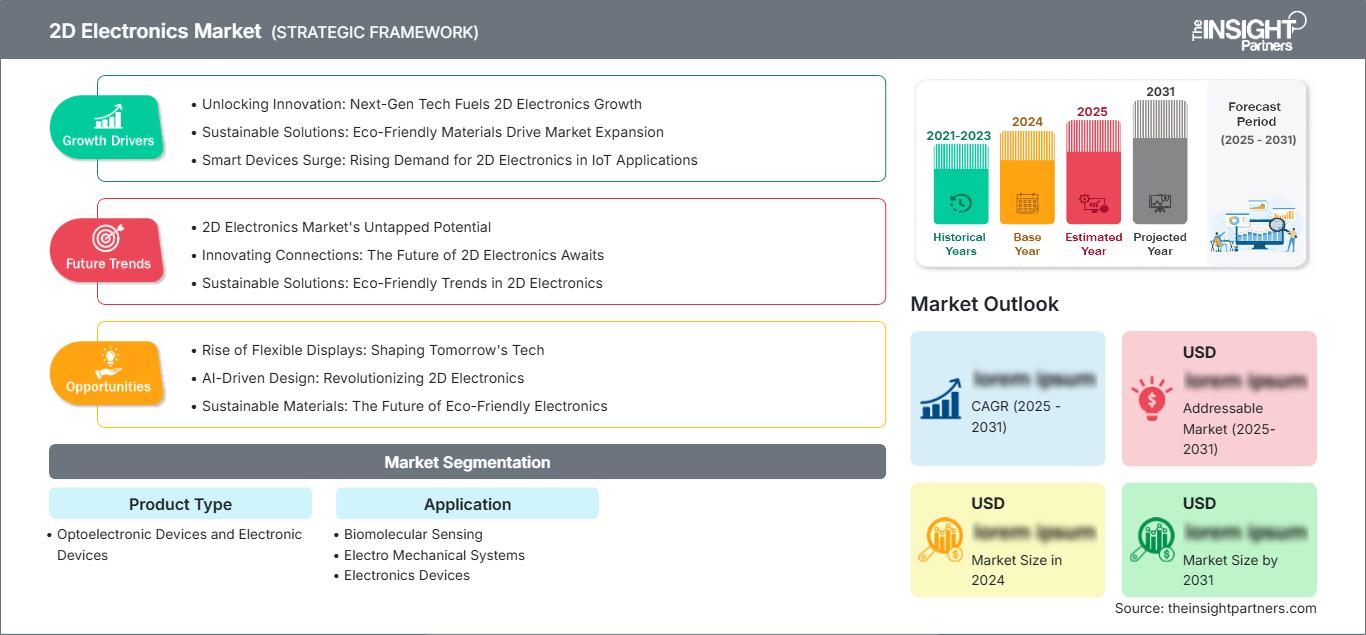
2D Electronics Market: Strategic Insights
Regional Insights
North America 2D Electronics Market
North America accounted for an estimated 24%–28% share in 2025 and is projected to expand at a CAGR of 8.4%–9.0%. The region is anchored by advanced semiconductor laboratories, medical technology clusters, and defense sensing programs that require compact, sensitive, and reliable electronic platforms. Demand is strongest for biomolecular sensing, optical communications, and security imaging, where 2D materials can improve detection surfaces, power efficiency, and device miniaturization.
Venture financing, technology spin-offs from universities, and domestic semiconductor efforts to qualify new material stacks have been used to facilitate commercialization. The share of the 2D Electronics Market in North America will remain stable due to customer demand for IP and customized manufacturing relationships. While adoption will be selective, niche applications such as health monitoring, photonics, aerospace electronics, and security infrastructure will support the use of high-cost materials and processes.
U.S. 2D Electronics Market
The U.S. represented 78%–82% of the North America 2D Electronics market size in 2025 and is expected to grow at a CAGR of 8.6%–9.2%. Its position reflects semiconductor design strength, national laboratory capability, and deep university research in atomically thin materials. Application demand is visible in photonic interconnects, flexible medical patches, secure imaging, and high-sensitivity biosensors, where performance validation can precede broad manufacturing scale.
The existence of companies makes it easier to go from material samples to prototype devices. Graphene Laboratories Inc., ACS Material, LLC, and 2D Semiconductors Inc. offer the supplies required for research and prototyping; however, the demand for these supplies comes from American-based electronics and medical device manufacturing companies. For the American market, commercialization is about proving reliability, protecting intellectual property, and collaborating with specialty manufacturers.
Europe 2D Electronics Market
Europe held an estimated 23%–27% of the 2D Electronics market share in 2025 and is forecast to grow at a CAGR of 8.7%–9.3%. Germany is the leading country because of its industrial electronics base, photonics ecosystem, and applied research institutes. The region benefits from coordinated advanced materials programs and demand for energy-efficient electronics in automotive, medical, and industrial automation applications.
The UK's contribution to the market is through graphene applications, the development of specialty materials, and translational research that bridges universities and industry. Haydale Graphene Industries plc adds value to the local materials pool via functionalized graphene technology, and device manufacturers seek opportunities in printed electronics, sensors, coating solutions, and flexible devices. The UK contribution is evident in areas where materials expertise is transferable to application technologies.
France is gaining visibility through Aledia SAS and microLED-related optoelectronic innovation, while Italy and Spain add value through research clusters, device engineering, and nanoscience capability. CIC nanoGUNE reinforces Spain’s position in advanced nanodevice research. These countries support the 2D Electronics Market trends around photonics, sensing, and flexible electronics, although manufacturing scale remains concentrated in selected industrial clusters.
APAC 2D Electronics Market
APAC led the global 2D Electronics Market with 38%–43% share in 2025 and is projected to grow at a CAGR of 9.4%–10.0%. China is the leading country, supported by semiconductor investment, display manufacturing, and materials research. Japan contributes precision materials and photonics capability, while South Korea strengthens demand through display and advanced electronics supply chains.
Relevance is increasing through growth in electronics fabrication, semiconductor strategy, and increased appetite for health technologies. Research on advanced materials and commercialization expertise is present in Australia. Strategies aimed at localizing semiconductor and display manufacturing make the case for using 2D materials even stronger for optoelectronic devices, sensors, and flexible electronics.
APAC's strength lies in its readiness for mass-scale manufacturing. Being able to incorporate new materials into existing devices faster than regions without downstream manufacturing capability means the region will succeed in using thin materials to increase brightness, sensitivity, conductivity, or flexibility without compromising manufacturing economics.
Middle East & Africa 2D Electronics Market
The Middle East & Africa 2D Electronics market is expected to grow at a CAGR of 7.8%–8.5%, from a smaller revenue base. Saudi Arabia is the leading country, supported by smart infrastructure, energy diversification, and industrial modernization. Demand is concentrated in sensors, energy systems, security technologies, and infrastructure monitoring rather than mass electronics manufacturing.
Innovation-driven pilot programs, smart cities, and research partnerships that enable photonics, sensing, and advanced manufacturing in the UAE have shown some progress. The possibilities in South Africa have been linked to mining, power supply, healthcare services, and industrial surveillance, all of which require rugged, mobile, and energy-efficient devices.
The use of RoMEA will depend on import alliances, reliability in the field, and cost-effective implementation. Energy and infrastructure environments offer opportunities for the deployment of sensing and energy-harvesting devices, where maintainability, grid stability, and environmental conditions influence purchase decisions.
Segmentation Analysis
Product Type
Product Type is expected to register a CAGR of 8.8%-9.4% during the period 2026-2034 as increasing acceptance in optoelectronics and electronics devices occurs. The optoelectronics applications include display technology, photodetectors, and optical communication. For electronics, the applications are sensor technology, transistors, flexible circuitry, and energy-related devices. The commercial success is dependent upon synthesis consistency and integration into the manufacturing line.
- Optoelectronic Devices: Optoelectronics are strategically important due to the use of enhancers that enable light emission, detection, modulation, and transparency in compact structures for use in displays, photodetectors, optical interconnections, and security imaging.
- Electronic Devices: Electronic devices have a wide range of applications for commercialization, including transistors, sensors, memory-proximity devices, flexible electronics, and conductive layers, all of which require ultrathin materials.
Application
Application is projected to grow at a CAGR of 9.3%–9.9% during 2026–2034 as end users prioritize flexible electronics, biomolecular sensing, optical communications, medical monitoring, and energy-linked devices. Application adoption is strongest where thinness, high surface sensitivity, transparency, and mechanical flexibility create measurable advantages over conventional materials. The 2D Electronics Market size expansion is therefore closely tied to device-specific qualification rather than generic material substitution.
- Biomolecular Sensing: Biomolecular sensing is strategically important because atomically thin surfaces respond strongly to molecular interactions, enabling compact diagnostics, wearable monitoring, and point-of-care detection with high surface sensitivity.
- Electro Mechanical Systems: Electro Mechanical Systems benefit from lightweight, responsive, and mechanically robust layers for miniature switches, resonators, and microsystems where surface behavior and dimensional scaling directly influence device performance.
- Electronics Devices: Electronics Devices support demand for low-power transistors, conductive films, sensors, and specialty components that address leakage, flexibility, high-frequency performance, and miniaturization challenges in advanced electronic architectures.
- Energy and Harvesting Devices: Energy and Harvesting Devices use 2D materials to enhance charge transport, interface control, and surface area utilization in supercapacitor-adjacent systems, thin-film storage, and self-powered distributed sensors.
- Medical Application: Medical Application demand is tied to conformable electronics, implant-adjacent systems, smart patches, and continuous monitoring devices where soft materials, signal fidelity, and low power consumption are essential.
- Optical Communications: Optical Communications is important because 2D materials can support compact photodetectors, modulators, and integrated photonic functions needed for faster, lower-power optical links and data-intensive infrastructure.
- Security Display and Imaging: Security Display and Imaging demand is linked to high-resolution sensors, secure displays, authentication systems, and detection platforms used across defense, infrastructure, and industrial inspection environments.
- Solar Cells Batteries: Solar Cells Batteries rely on 2D materials for transparent electrodes, interface engineering, charge management, and flexible power architectures that support lightweight energy conversion and storage formats.
- Flexible Electronics: Flexible Electronics is the leading application because conductivity, transparency, and bendability enable wearables, foldable displays, electronic skin, smart labels, and compact sensors with clear product differentiation.
Opportunity Snapshot
| Application | Revenue Contribution | Trend Tag | Adoption Stage |
| Biomolecular Sensing | Medium | Rapid Tests | Scaling |
| Electro-Mechanical Systems | Low | Micro Actuation | Emerging |
| Electronics Devices | High | Low Power | Scaling |
| Energy and Harvesting Devices | Medium | Self Power | Emerging |
| Medical Application | Medium | Smart Patches | Scaling |
| Optical Communications | Medium | Optical Links | Scaling |
| Security Display and Imaging | Medium | Secure Imaging | Emerging |
| Solar Cells Batteries | Medium | Thin Power | Emerging |
| Flexible Electronics | High | Foldable Devices | Mature |
2D Electronics Market Growth Drivers and Impact Analysis
Post-silicon device scaling requirements
Semiconductor developers are evaluating 2D materials because conventional scaling faces power, heat, and leakage constraints as device architectures become smaller and denser. Atomically thin channels are characterized by strong electrostatic effects, while selected transition-metal dichalcogenides exhibit a band gap, making them suitable for logic and optoelectronic applications. The true market effect will not be to replace silicon immediately, but rather to insert selectively into valuable device layers where thinness, reduced leakage, or surface control will make a difference. This provides room for collaboration among materials providers, fabs, and device companies on qualification-ready prototypes and strengthens the long-term growth in the 2D Electronics Market.
Flexible and conformable device demand
Flexible electronics provide one of the clearest commercial pathways because 2D materials can combine conductivity, mechanical flexibility, transparency, and low thickness in a single device layer. Wearable sensors, foldable displays, smart labels, soft medical patches, and electronic skin require materials that perform under bending or conformal contact. The market impact extends beyond material sales, as adoption also drives demand for encapsulation, printing, transfer, and low-temperature processing. OEMs gain product differentiation through lighter, thinner, and more comfortable devices, which makes flexible electronics the largest application area in the 2D Electronics Market.
High-sensitivity sensing and photonics adoption
There is an increased need for sensing and photonics applications because 2D materials exhibit a high surface-to-volume ratio, fast optical response times, and tunable electronic properties. Sensors that utilize biomolecules could benefit from surface-level interactions, whereas photodetectors and optical communication devices may take advantage of thinner layers in the active area to reduce size and power consumption. The greatest commercial relevance will be seen in diagnostics, security imaging, and data-centric infrastructures due to the ability to estimate performance improvements, which leads to increased value in pricing and validation.
2D Electronics Market Future Trends
Wafer-scale process control becomes a differentiator
A defining future trend is the movement from laboratory material performance to wafer-scale process control. Device makers require uniform thickness, low defect density, stable transfer, and compatibility with lithography and packaging workflows. As 2D materials move closer to commercial qualification, companies that demonstrate repeatable deposition and integration will gain stronger bargaining power than firms offering only research-grade samples. These 2D Electronics market trends will influence supplier selection in displays, photonics, and specialty semiconductors because customers need predictable yields before committing capital to production programs.
Application-specific heterostructures gain relevance
2D Electronics technology is transitioning from a single-material story to one in which heterostructures composed of graphene, transition metal dichalcogenides, boron nitride, and other thin materials work together to achieve desired performance. Such a combination of materials enables the designer to tailor the electronic bandgap, conductivity, optical properties, barrier properties, and thermal behavior to the specific application. The commercial success of the future will lie in application-ready material stacks that solve specific engineering challenges, rather than in new materials.
2D Electronics Market Opportunities
Co-development with display and photonics manufacturers
Co-development with display, microLED, and photonics manufacturers is one of the most actionable opportunities because these customers already invest in advanced materials to improve brightness, efficiency, resolution, and optical performance. Supporting the 2D electronics market forecast, 2D material companies should be able to minimize the risk associated with commercialization by focusing on specific device characteristics rather than overall platform characteristics. Pilot production lines, qualification efforts, and supply contracts can help generate early revenue and validate manufacturing feasibility. The most promising cases are those in which thin materials improve performance without disrupting existing manufacturing infrastructure.
Portable diagnostics and medical wearables
Portability of medical devices provides a compelling business case, as it favors sensitivity, adaptability, reduced energy consumption, and small form factors. 2D materials have applications in the development of smart patches, biosensors, and point-of-care devices for operations outside clinical facilities. Investors should look at businesses where the material capabilities are complemented by encapsulation, biocompatibility research, data processing, and manufacturing scalability. The business case is compelling because certain healthcare use cases can command higher prices when devices provide high-quality data, comfort, or faster testing workflows.
Recent Developments
- June 2026: Skeleton Technologies GmbH launched GrapheneUPS, a high-density uninterruptible power supply platform for AI data centers using its curved graphene-based energy storage technology. The announcement is relevant because it links graphene-derived materials with power-critical electronics infrastructure, where response speed, reliability, and energy efficiency are core purchasing criteria.
- May 2026: Aledia SAS announced a strategic partnership with AUO Corporation to develop next-generation low-power, high-brightness microLED displays by combining Aledia’s high-voltage microLED technology and AUO’s display backplane expertise. The project supports industrialization of advanced display technologies and adjacent optical interconnect applications.
- December 2025: The 2D Pilot Line (2D-PL), a Graphene Flagship initiative focused on advancing the industrial adoption of graphene and other two-dimensional (2D) materials for semiconductor applications, has launched its fourth multi-project wafer (MPW) run. This milestone further strengthens Europe’s capabilities in prototyping and fabricating semiconductor devices based on graphene and other 2D materials.
Frequently Asked Questions

- Comprehensive Market Sizing and Forecast Analysis
- Detailed Segmentation Analysis
- In-Depth Market Dynamics Assessment
- Regional and Country-Level Insights
- Competitive Landscape and Company Benchmarking
- Strategic Business Intelligence
Recent Reports
Testimonials

The Insight Partners' SCADA System Market report is comprehensive, with valuable insights on current trends and future forecasts. The team was highly professional, responsive, and supportive throughout. We are very satisfied and highly recommend their services.
RAN KEDEM Partner, Reali Technologies LTDs
I requested a report on a very specific software market and the team produced the report in a few days. The information was very relevant and well presented. I then requested some changes and additions to the report. The team was again very responsive and I got the final report in less than a week.
JEAN-HERVE JENN Chairman, Future Analytica
We worked with The Insight Partners for an important market study and forecast. They gave us clear insights into opportunities and risks, which helped shape our plans. Their research was easy to use and based on solid data. It helped us make smart, confident decisions. We highly recommend them.
PIYUSH NAGPAL Sr. Vice President, High Beam Global
The Insight Partners delivered insightful, well-structured market research with strong domain expertise. Their team was professional and responsive throughout. The user-friendly website made accessing industry reports seamless. We highly recommend them for reliable, high-quality research services
YUKIHIKO ADACHI CEO, Deep Blue, LLC.
This is the first time I have purchased a market report from The Insight Partners.While I was unsure at first, I visited their web site and felt more comfortable to take the risk and purchase a market report.I am completely satisfied with the quality of the report and customer service. I had several questions and comments with the initial report, but after a couple of dialogs over email with their analyst I believe I have a report that I can use as input to our strategic planning process.Thank you so much for taking the extra time and making this a positive experience.I will definitely recommend your service to others and you will be my first call when we need further market data.
JOHN SUZUKI President and Chief Executive Officer, Board Director, BK Technologies
I wish to appreciate your support and the professionalism you displayed in the course of attending to my request for information regarding to infectious disease IVD market in Nigeria. I appreciate your patience, your guidance, and the fact that you were willing to offer a discount, which eventually made it possible for us to close a deal. I look forward to engaging The Insight Partners in the future, all thanks to the impression you have created in me as a result of this first encounter.
DR CHIJIOKE ONYIA MANAGING DIRECTOR, PineCrest Healthcare Ltd.Reason to Buy
- Informed Decision-Making
- Understanding Market Dynamics
- Competitive Analysis
- Identifying Emerging Markets
- Customer Insights
- Market Forecasts
- Risk Mitigation
- Boosting Operational Efficiency
- Strategic Planning
- Investment Justification
- Tracking Industry Innovations
- Aligning with Regulatory Trends





 Get Free Sample for