
Acoustic Microscopy Market Growth, Trends & Forecast by 2034
Coverage: by Offering (Microscopes, Accessories and Software, Services); Application (Non-Destructive Testing, Failure Analysis, Product Reliability Testing/Quality Control, Others); Industry Vertical (Semiconductor, Life Science, Material Science, Nanotechnology, Others) , and Geography (North America, Europe, Asia Pacific, and South and Central America)
- Status : Data Released
- Report Code : TIPRE00011478
- Category : Electronics and Semiconductor
- No. of Pages : 150
- Available Report Formats :


- Last update date : July 14, 2026


2025 Market Size
US$ 718.95 Mn
Base year value
2034 Forecast
US$ 1,237.65 Mn
Projected by 2034
CAGR 2026-2034
6.22 %
Growth rate
Addressable Market
US$ 8,855.86 Mn
(2026-2034)
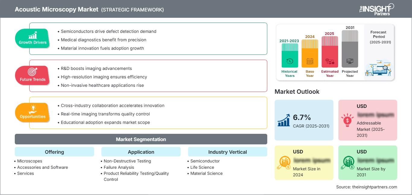
The Acoustic Microscopy Market was valued at US$ 718.95 Million in 2025 and is projected to reach US$ 1,237.65 Million by 2034, expanding at a CAGR of 6.22% during 2026–2034. Acoustic microscopy uses high-frequency ultrasound to inspect internal structures, interfaces, voids, cracks, delamination, and bonding defects without damaging precision components across semiconductor, life science, material science, and nanotechnology applications.
North America is expected to record a CAGR range of 5.6–6.0% during 2026–2034, supported by semiconductor packaging reliability programs, aerospace materials inspection, and outsourced failure-analysis laboratories. Growth is reinforced by advanced packaging investment, medical-device qualification, and greater use of non-destructive testing where destructive cross-sectioning is costly, slow, or unsuitable for high-value components.
Acoustic Microscopy Market Assessment and Insights
- North America: 29–33% share in 2025 and CAGR between 2026–2034 of 5.6–6.0%; demand is led by semiconductor reliability, aerospace composites, medical devices, and contract failure-analysis laboratories.
- US: 78–82% of North America share in 2025 and CAGR between 2026–2034 of 5.5–5.9%; advanced packaging, defense electronics, and outsourced analytical services sustain adoption.
- Europe: 22–26% share in 2025 and CAGR between 2026–2034 of 5.3–5.7%; Germany, the UK, France, Italy, and Spain lead through materials research, automotive electronics, and industrial quality programs.
- Asia Pacific: 34–38% share in 2025 and CAGR between 2026–2034 of 6.8–7.2%; China, Japan, South Korea, India, and Taiwan benefit from semiconductor, electronics, and advanced materials production.
- Largest Segment: Microscopes held 48–52% market share in 2025, CAGR range 5.8–6.2%, supported by semiconductor labs, quality-control departments, and research institutes.
- High Growth Segment: Services held 18–22% market share in 2025, CAGR range 7.0–7.4%, driven by outsourcing, limited in-house expertise, and recurring failure-analysis workloads.
- Key companies analyzed in detail: Accurex Solutions Pvt. Ltd.; EAG Laboratories; Hitachi High-Tech Corporation; Insight K.K.; IP-holding GmbH; MuAnalysis Inc.; Element Materials Technology Group Limited; OKOS Solutions, LLC; PVA TePla AG; Sonix Inc.
Source: The Insight Partners' analysis based on proprietary research, government publications, company annual reports, investor presentations, industry databases, and expert interviews.
The acoustic microscopy market report has moved from laboratory-based inspection toward automated, production-adjacent metrology for advanced packages, bonded wafers, composites, and biomaterials. Higher-frequency transducers, faster scanning stages, improved time-of-flight tools, and image-analysis software are reshaping production dynamics. Manufacturers increasingly deploy acoustic systems to detect hidden voids and delamination before final assembly, reducing destructive testing, scrap, and qualification delays in complex electronic and material structures.
Forward growth will be shaped by Asia Pacific semiconductor capacity, North American analytical-service demand, and European materials-engineering programs. Regulatory emphasis on device reliability, traceable quality systems, and safer non-destructive testing methods supports adoption. As electronics, aerospace, medical devices, and nanotechnology products become thinner, stacked, and more heterogeneous, acoustic microscopy market growth will depend on resolution, automation, software interpretation, and application support.
Acoustic Microscopy Market Report Scope
| Report Attribute | Details |
|---|---|
| Market size in 2025 | US$ 718.95 Million |
| Market Size by 2034 | US$ 1,237.65 Million |
| Global CAGR (2026 - 2034) | 6.22% |
| Historical Data | 2021-2024 |
| Forecast period | 2026-2034 |
Acoustic Microscopy Market Analysis
Demand is anchored in the need to inspect sealed, opaque, and multilayer components without destroying them. Semiconductor packaging, wafer bonding, MEMS, power electronics, composites, and medical materials require identification of cracks, voids, disbonds, inclusions, and delamination at early process stages. The Acoustic Microscopy Market analysis reflects rising preference for internal defect visibility, depth profiling, and repeatable quality evidence.
The ecosystem includes transducer suppliers, microscope manufacturers, software developers, calibration specialists, analytical laboratories, semiconductor fabs, research institutes, and quality-control teams. Supply dynamics depend on piezoelectric materials, precision motion systems, immersion handling, digitizers, and application libraries. The acoustic microscopy market size expands as buyers require both capital equipment and services that convert acoustic signatures into actionable reliability decisions.
The competitive landscape combines specialist system vendors, diversified metrology companies, and service laboratories. PVA TePla AG, Sonix Inc., Hitachi High-Tech Corporation, OKOS Solutions, LLC, and Insight K.K. compete on resolution, throughput, automation, and software interpretation. EAG Laboratories, MuAnalysis Inc., and Element Materials Technology Group Limited strengthen market access through outsourced analysis for electronics, aerospace, and regulated industrial customers.
Investment trends favor automated wafer inspection, high-frequency transducers, AI-assisted defect classification, and connected service models. Strategic positioning increasingly depends on application expertise rather than hardware specifications alone. Vendors that support advanced packaging, hybrid bonding, composite qualification, and biomedical materials can improve Acoustic Microscopy market share by lowering interpretation barriers and shortening root-cause analysis cycles.
● REPORT CUSTOMIZATION
Tailor This Report To Align With Your Specific Business Requirements
This report can be customized to align precisely with your business objectives, scope, and target markets. Customization options include tailored segmentation, geography, competitive analysis, and strategic insights to support informed decision-making.
Customize This Report →WHAT YOU CAN ADJUST
- ● Segmentations
- ● Geography
- ● Competitive Analysis
- ● Language Preferences
Acoustic Microscopy Market: Strategic Insights
Regional Insights
North America Acoustic Microscopy Market
North America accounted for 29–33% share in 2025 and is expected to grow at a CAGR of 5.6–6.0% during 2026–2034. Semiconductor packaging, aerospace composites, defense electronics, and medical-device validation drive inspection requirements. Acoustic systems help laboratories detect buried defects that are not visible through optical inspection and may be missed by conventional radiography.
Regional demand is driven by outsourced analysis testing, robust university research, and qualification standards in heavily regulated supply chains. Repeatability, depth resolution, and documentation for corrective action are crucial for buyers. The scope of the Acoustic Microscopy market is expanding due to the need for non-destructive analysis of the interiors of complex devices such as advanced packaging, batteries, MEMS, and implantable device components, which require internal inspection before reliability testing.
U.S. Acoustic Microscopy Market
The U.S. represented 78–82% of North America share in 2025 and is projected to expand at a CAGR of 5.5–5.9% through 2034. Demand is concentrated in advanced packaging, aerospace electronics, power modules, medical devices, and third-party failure-analysis laboratories. Sonix Inc., EAG Laboratories, MuAnalysis Inc., and OKOS Solutions, LLC maintain meaningful technology or service presence.
Application trends include bonded wafer testing, package delamination mapping, counterfeiting detection, and mission-critical component qualification. Market drivers include the United States' advantages in electronics reshoring initiatives, defense reliability initiatives, and high-value analysis offerings. Another trend in the acoustic microscopy market includes increased use of digital imaging databases, recipe automation, and defect libraries for recurring production problems.
Europe Acoustic Microscopy Market
Europe held 22–26% share in 2025 and is forecast to grow at a CAGR of 5.3–5.7% during 2026–2034. Germany leads regional adoption through automotive electronics, compound semiconductors, industrial materials, and applied research. German buyers typically value repeatable imaging, equipment uptime, calibration discipline, and integration into structured quality-management systems.
The United Kingdom has a market that uses aerospace composites, nanotechnology centers at universities, and laboratories for electronics reliability, which together generate demand. France has benefited from aerospace, defense, and microelectronics programs, while Italy has used acoustic microscopy in industrial materials, power electronics, and specific manufacturing processes. Although Spain has been relatively small in this industry, it benefits from research centers, automotive parts makers, and component testing in renewable energy.
European adoption is driven by traceability needs, safety product concerns, and investment in local semiconductor capabilities. PVA TePla AG and Hitachi High-Tech Corporation remain relevant, while service laboratories help clients lacking in-house systems. The share of the acoustic microscopy market increases when no other means of preserving evidence exist during destructive sectioning.
APAC Acoustic Microscopy Market
APAC accounted for 34–38% share in 2025 and is expected to post a CAGR of 6.8–7.2% through 2034. China leads through electronics manufacturing, packaging expansion, and materials laboratories.
Japan and South Korea focus on wafer bonding, MEMS, power devices, and quality systems in advanced electronics. India leverages outsourcing engineering services, medical devices, and semiconductor policy programs to increase demand.
Taiwan and Australia include demand for semiconductor packaging, research, and materials testing. Industrial policy, electronics exports, and failure analysis capability make the Asia-Pacific the fastest-growing region for adoption of the Acoustic Microscopy Market.
Middle East & Africa Acoustic Microscopy Market
Middle East & Africa acoustic microscopy market is projected to grow at a CAGR of 4.7–5.1% during 2026–2034. Saudi Arabia drives demand through research universities, energy materials and electronics initiatives, and industrial diversification programs.
The UAE offers support for adoption in aerospace maintenance, advanced manufacturing, and labs in technology zones, whereas South Africa provides mining products, academic research, and industrial inspections. Other MEAs are service-oriented.
The need for energy infrastructure, harsh-environment products, and QA necessitates this adoption; however, high cost and a lack of acoustic imaging experts hamper faster adoption. Partnerships in services are crucial for regional adoption.
Segmentation Analysis
Offering
The offering segment is projected to grow at a CAGR of 6.0–6.4% during 2026–2034. Microscopes remain the capital-equipment anchor, while accessories and software improve resolution, data handling, and repeatability. Services expand as companies outsource failure analysis, recipe development, training, and overflow inspection when internal laboratories face capacity or expertise constraints.
- Microscopes represent the core revenue base, serving semiconductor, materials, and research laboratories that require controlled scanning, high-frequency transducers, and repeatable internal defect visualization.
- Accessories and Software strengthen installed systems through probes, digitizers, fixtures, image-processing tools, and automated analysis, helping users improve throughput, documentation, and interpretation consistency.
- Services address customers that need failure analysis, method development, calibration, maintenance, or overflow scanning without committing immediately to full in-house acoustic microscopy infrastructure.
Application
The application segment is expected to grow at a CAGR of 6.1–6.5% during 2026–2034. Non-destructive testing leads because customers need internal inspection before destructive validation. Failure analysis remains essential for root-cause investigations, while product reliability testing and quality control support production release, supplier qualification, and corrective-action programs across high-value components.
- Non-Destructive Testing is the principal use case, enabling internal inspection of sealed, bonded, or multilayer components while preserving samples for downstream electrical, mechanical, or reliability evaluation.
- Failure Analysis supports root-cause investigation after field returns, yield loss, or qualification failures, helping engineers isolate delamination, cracks, voiding, weak bonds, and process-induced defects.
- Product Reliability Testing/Quality Control applies acoustic inspection to incoming materials, process validation, and final release, improving documentation, repeatability, and supplier accountability for critical products.
Industry Vertical
The industry vertical segment is forecast to grow at a CAGR of 6.2–6.6% during 2026–2034. Semiconductor remains the most commercially significant vertical, while life science, material science, and nanotechnology expand use cases for soft tissue, biomaterials, composites, thin films, and microstructures. Adoption improves where inspection must preserve samples and reveal subsurface discontinuities.
- Semiconductor demand is driven by advanced packaging, wafer bonding, MEMS, power devices, and package reliability programs that require precise internal defect mapping before production release.
- Life Science applications include biomaterials, medical-device interfaces, tissue scaffolds, and implant structures where non-destructive imaging helps evaluate bonding, voids, and material uniformity.
- Material Science uses acoustic inspection for composites, ceramics, polymers, metals, coatings, and bonded assemblies, supporting research, failure analysis, and production-quality decisions.
- Nanotechnology adoption is emerging in thin films, microstructures, and layered materials, where small defects can influence performance, reliability, and process repeatability.
Opportunity Snapshot
| Industry Vertical | Revenue Contribution | Trend Tag | Adoption Stage |
| Semiconductor | High | Advanced Packaging | Mature |
| Life Science | Medium | Biomaterial Imaging | Scaling |
| Material Science | High | Composite Integrity | Mature |
| Nanotechnology | Medium | Thin Films | Emerging |
| Others | Low | Specialty Testing | Emerging |
Acoustic Microscopy Market Growth Drivers and Impact Analysis
Advanced Packaging Raises Internal Defect Visibility Requirements
The more sophisticated the semiconductor package design, the more difficult it is to inspect such packages for die stacking, underfill, redistribution layer, micro-bump formation, and bonding interface issues using only surface inspection techniques. Acoustic microscopy is used to non-destructively assess delamination, voiding, cracks, and weak bonds before expensive further processing or qualification. This technology has its greatest impact on the markets for outsourced semiconductor assembly, wafer-level packaging, MEMS, and power electronics, where reliability failures can affect automotive, industrial, and communications applications.
Regulated Products Demand Stronger Reliability Evidence
Medical equipment, aerospace parts, military electronics, and process control units need verification that the presence of flaws is under control before product shipment. Acoustic microscopy allows for non-destructive traceability inspection of expensive samples; it is appropriate for supplier certification, remedial actions, and lot release. The technology goes beyond flaw detection since stored acoustic images can be used by engineers to compare different processes, verify bonding, and evaluate field returns. This strengthens adoption among manufacturers that must balance reliability requirements, limited sample availability, and the need for repeatable quality records.
Outsourced Failure Analysis Expands Access to Expertise
Many companies will only occasionally require acoustic inspection and thus cannot afford to invest in equipment, personnel, and method development at that time. Laboratory services broaden access to these services by offering scanning, analysis, cross-validation, and reporting for failure analysis, supplier disputes, and emergencies in the manufacturing process. This is especially crucial for small electronics, materials, and medical devices companies, which require proof but lack in-house acoustic inspection capabilities. The service providers will train their clients, paving the way for eventual equipment purchases.
Acoustic Microscopy Market Future Trends
AI-Assisted Acoustic Image Interpretation Becomes Standard
Machine learning technology will be widely used in future acoustic microscopy systems to categorize voids, delaminations, cracks, inclusions, and variations in bond quality, using large datasets collected during inspection operations. This will limit the reliance on rare experts and ensure consistent analysis across different locations, shifts, and product lines. It is anticipated that AI-powered processes will incorporate acoustic imaging data, process data, electrical test results, and reliability metrics, thereby providing predictive feedback for manufacturing teams.
Automated High-Throughput Inspection Moves Closer to Production
There will be an even greater shift away from offline analytical labs and towards more production-oriented areas that prioritize repeatability, recipes, and throughput. The automated sample loading, field scanning size, wafer handling, defect level, and statistics will assist the user in screening more wafers without compromising the production process. This development will be crucial in areas such as advanced packaging, power modules, and bonding applications, where sampling alone might not detect deviations from the process. Integration with manufacturing execution systems will allow acoustic results to support faster release, rework, or process-adjustment decisions.
Acoustic Microscopy Market Opportunities
Expansion of Non-Destructive Testing in Advanced Semiconductor Packaging
The rapid adoption of advanced semiconductor packaging technologies, including 2.5D/3D ICs, chiplets, wafer-level packaging, and heterogeneous integration, is creating significant opportunities for acoustic microscopy vendors. High-resolution, non-destructive testing methods are needed by manufacturers to detect delaminations, voids, cracks, and bonding issues before final assembly. Suppliers can grow by supplying automated acoustic microscopy systems with AI-enabled defect detection, high scan rates, and seamless integration into the semiconductor manufacturing process. Increased investment in chip fabrication and packaging plants supports the acoustic microscopy market forecast.
Service-Based Inspection and Predictive Failure Analysis
Acoustic microscopy vendors have an opportunity to sustain revenue by offering more services, including inspection-as-a-service, preventive maintenance, calibration, software upgrades, and predictive failure analysis. For many manufacturers of medical devices, electronics, and aerospace components, and research institutions, inspection services offered on a per-project basis are more cost-effective than purchasing expensive imaging systems. Services such as cloud-based reporting, digital imaging storage, artificial intelligence-based defect classifications, and lifecycle management help retain customers and keep costs down for end users.
Recent Developments
- August 2025: Nordson Test & Inspection announced plans to unveil advanced technology at SEMICON Taiwan, scheduled to take place at TaiNex in Taipei at booth #12326. The company will demonstrate state-of-the-art Optical, X-Ray and Acoustic Inspection and Metrology systems and unveil the new Auto Centering Sensor (ACS). Additionally, across technology platforms, the advanced Nordson Intelligence AI Ecosystem will be featured. Nordson Test & Inspection is a platinum sponsor.
- February 2025: Leica Microsystems, a leader in microscopy and scientific instrumentation and advanced imaging solutions, announced that it has acquired ATTO-TEC, a leading specialty supplier of fluorescent dyes and reagents. The addition of dyes and reagents for sample preparation complements the renowned Leica portfolio of microscopy imaging platforms and advanced AI-based analysis software.
- October 2025: Hitachi High-Tech India Pvt. Ltd., a subsidiary of Hitachi High-Tech Corporation Japan, inaugurated an avant-garde Technology and Innovation Center in Bengaluru, underscoring the company’s strategic commitment to India’s accelerating high-technology renaissance. The facility is conceived as a catalytic hub of scientific convergence, integrating semiconductor research, advanced materials innovation, and cross-disciplinary industrial applications under one ecosystem. Outfitted with state-of-the-art analytical instrumentation and nanotechnological characterization capabilities, the center will facilitate experiential demonstrations, joint research engagements, and accelerated prototype validation for academia, manufacturing, and energy-storage domains.
Frequently Asked Questions

- Comprehensive Market Sizing and Forecast Analysis
- Detailed Segmentation Analysis
- In-Depth Market Dynamics Assessment
- Regional and Country-Level Insights
- Competitive Landscape and Company Benchmarking
- Strategic Business Intelligence
Recent Reports
Testimonials

The Insight Partners' SCADA System Market report is comprehensive, with valuable insights on current trends and future forecasts. The team was highly professional, responsive, and supportive throughout. We are very satisfied and highly recommend their services.
RAN KEDEM Partner, Reali Technologies LTDs
I requested a report on a very specific software market and the team produced the report in a few days. The information was very relevant and well presented. I then requested some changes and additions to the report. The team was again very responsive and I got the final report in less than a week.
JEAN-HERVE JENN Chairman, Future Analytica
We worked with The Insight Partners for an important market study and forecast. They gave us clear insights into opportunities and risks, which helped shape our plans. Their research was easy to use and based on solid data. It helped us make smart, confident decisions. We highly recommend them.
PIYUSH NAGPAL Sr. Vice President, High Beam Global
The Insight Partners delivered insightful, well-structured market research with strong domain expertise. Their team was professional and responsive throughout. The user-friendly website made accessing industry reports seamless. We highly recommend them for reliable, high-quality research services
YUKIHIKO ADACHI CEO, Deep Blue, LLC.
This is the first time I have purchased a market report from The Insight Partners.While I was unsure at first, I visited their web site and felt more comfortable to take the risk and purchase a market report.I am completely satisfied with the quality of the report and customer service. I had several questions and comments with the initial report, but after a couple of dialogs over email with their analyst I believe I have a report that I can use as input to our strategic planning process.Thank you so much for taking the extra time and making this a positive experience.I will definitely recommend your service to others and you will be my first call when we need further market data.
JOHN SUZUKI President and Chief Executive Officer, Board Director, BK Technologies
I wish to appreciate your support and the professionalism you displayed in the course of attending to my request for information regarding to infectious disease IVD market in Nigeria. I appreciate your patience, your guidance, and the fact that you were willing to offer a discount, which eventually made it possible for us to close a deal. I look forward to engaging The Insight Partners in the future, all thanks to the impression you have created in me as a result of this first encounter.
DR CHIJIOKE ONYIA MANAGING DIRECTOR, PineCrest Healthcare Ltd.Reason to Buy
- Informed Decision-Making
- Understanding Market Dynamics
- Competitive Analysis
- Identifying Emerging Markets
- Customer Insights
- Market Forecasts
- Risk Mitigation
- Boosting Operational Efficiency
- Strategic Planning
- Investment Justification
- Tracking Industry Innovations
- Aligning with Regulatory Trends





 Get Free Sample for