
Epitaxy Growth Equipment Market Size, Share & Demand by 2034
Coverage: By Product (LED, Laser Diode, RF Equipment, MEMS); Application (Photonics, Semiconductor, Wide-band Gap Material, Others), and Geography (North America, Europe, Asia Pacific, and South and Central America)
- Status : Data Released
- Report Code : TIPRE00018380
- Category : Electronics and Semiconductor
- No. of Pages : 150
- Available Report Formats :


- Last update date : August 26, 2026


2025 Market Size
US$ 1.64 Bn
Base year value
2034 Forecast
US$ 3.20 Bn
Projected by 2034
CAGR 2026-2034
7.71 %
Growth rate
Addressable Market
US$ 21.79 Bn
(2026-2034)
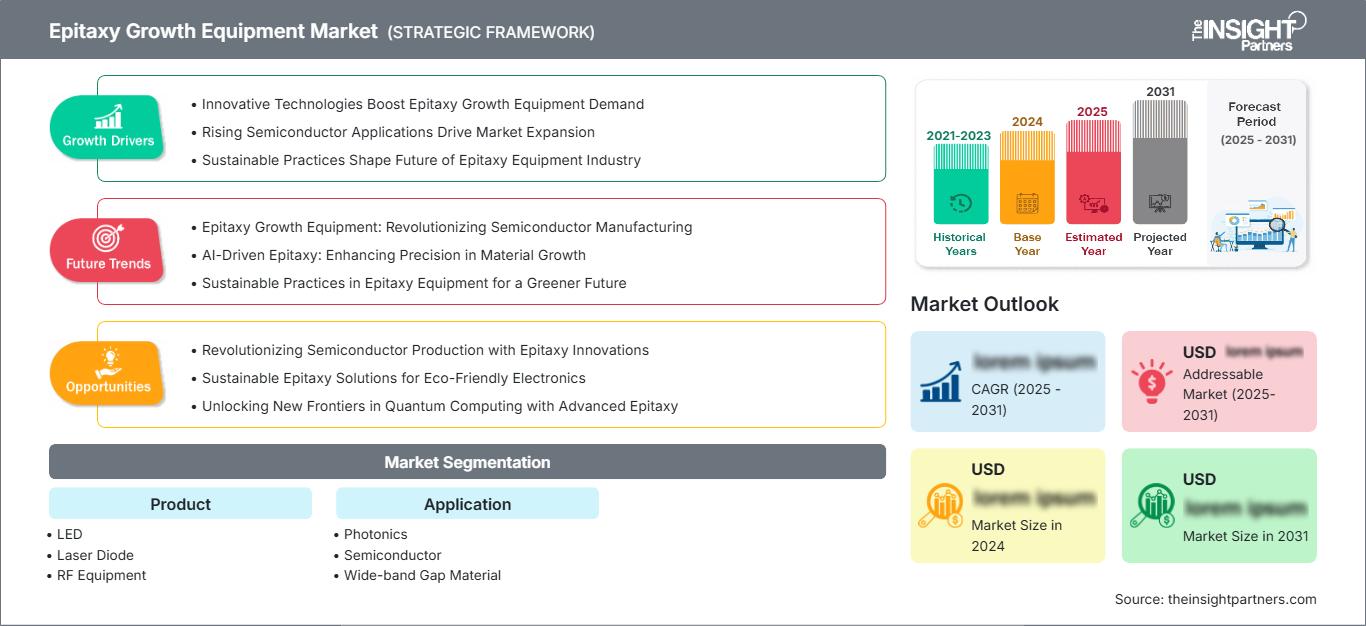
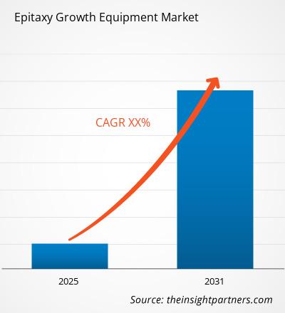
The Epitaxy Growth Equipment Market was valued at US$ 1.64 Billion in 2025 and is projected to reach US$ 3.20 Billion by 2034, registering a CAGR of 7.71% during 2026–2034. Expansion is being shaped by increasing semiconductor complexity, wider deployment of compound semiconductor devices, and greater investment in photonics, RF, and wide-bandgap manufacturing. Equipment suppliers are responding through higher wafer throughput, tighter epitaxial-layer control, improved automation, and greater process flexibility across demanding production environments.
The Epitaxy Growth Equipment Market size is increasingly influenced by North American semiconductor capacity expansion, particularly investments in advanced logic, memory, RF, and compound semiconductor manufacturing. The regional outlook is supported by domestic supply-chain initiatives, fab construction, and demand for GaN and SiC technologies. These structural factors indicate an estimated 7.2–7.9% CAGR through 2034, with capital-intensive projects encouraging suppliers to strengthen local technical support, process qualification capabilities, and production scalability.
Epitaxy Growth Equipment Market Assessment and Insights
- North America: North America represented a 16–18% Epitaxy Growth Equipment Market share in 2025 and is estimated to grow at a 7.2–7.9% CAGR during 2026–2034, supported by semiconductor localization, compound semiconductor capacity, and advanced-device investment.
- US: The US accounted for 80–84% of North America's 2025 market, with a 7.4–8.0% CAGR projected through 2034 as domestic fab investment expands equipment requirements.
- Europe: Europe held a 17–19% share in 2025 and is projected to grow at a 6.8–7.5% CAGR, led by Germany, France, Italy, and the UK across power, automotive, and photonics applications.
- Asia Pacific: Asia Pacific commanded a 59–62% share in 2025 and is expected to expand at an 8.0–8.8% CAGR, led by China, Japan, South Korea, and increasingly India.
- Largest Segment: Semiconductor applications represented a 38–42% market share in 2025 and are expected to grow at a 7.8–8.3% CAGR through 2034.
- High Growth Segment: Wide-band Gap Material applications held a 22–26% market share in 2025 and are projected to register an 11.5–12.5% CAGR during 2026–2034.
- Key companies analyzed in detail: AIXTRON SE, Advanced Micro-Fabrication Equipment Inc. China, Applied Materials, Inc., Wolfspeed, Inc., DOWA Electronics Materials Co., Ltd., DuPont de Nemours, Inc., Epiworks, Inc., Coherent Corp., Intelligent Epitaxy Technology, Inc., and Optowell Co., Ltd.
Source: The Insight Partners' analysis based on proprietary research, government publications, company annual reports, investor presentations, industry databases, and expert interviews.
The Epitaxy Growth Equipment Market has moved away from being centered on equipment designed specifically for LED and compound semiconductor fabrication into tools that can accommodate increasing complexity in terms of epitaxial structures. Larger wafer sizes, selective deposition, better thickness control, automation of processes, and enhanced defect control will influence economic dynamics of reactors. Multi-material capability and repeatable recipes are key for suppliers, while yield, qualifications and cost-per-wafer are key considerations for customers.
The Epitaxy Growth Equipment Market trends indicate that investments in epitaxial reactors are expected to diversify beyond traditional production sites in Asia due to growing semiconductor ecosystem in North America, Europe and India. Development programs in chip fabs, photonics, and wide band-gap materials are anticipated to drive local equipment purchases. Market prospects are affected by demands for high-frequency and high-power devices where epitaxial layer quality is critical for performance, heat dissipation and yields.
Epitaxy Growth Equipment Market Report Scope
| Report Attribute | Details |
|---|---|
| Market size in 2025 | US$ 1.64 Billion |
| Market Size by 2034 | US$ 3.20 Billion |
| Global CAGR (2026 - 2034) | 7.71% |
| Historical Data | 2021-2024 |
| Forecast period | 2026-2034 |
Epitaxy Growth Equipment Market Analysis
Epitaxy Growth Equipment market is very dependent on the cost of semiconductor fabrication since the epitaxial layers determine how the carriers will perform and also how they will behave in breakdown conditions. Applications for this equipment include LEDs, laser diodes, RF applications, MEMS, and advanced power devices that have a diverse customer base. The supply chain includes substrate suppliers, precursors suppliers, reactors, metrology tools, end users, and foundry services.
Along the supply chain, vendors increasingly incorporate process monitoring into their reactor platform. SiC and GaN require the need to have high-temperature capabilities, defect mitigation, and thick layer formation while photonics requires accuracy in compositions and interfaces. The purchase of the equipment relies on application economics, utilization rates, size of substrate used, wafer throughput, and process recipe qualification capability of the customer.
In terms of competitive position, Epitaxy Growth Equipment market is comprised of specialized deposition firms alongside general semiconductor equipment providers. In terms of competitive exposure to the sector, AIXTRON SE has considerable exposure to compound semiconductor deposition, while Applied Materials, Inc. competes in the segment via its advanced epitaxy platforms for logic and memory. Coherent Corp. is exposed to materials, epitaxy, and photonics, while DOWA Electronics Materials Co., Ltd. has involvement in gallium-based materials and epitaxial substrates.
Competitive positioning is becoming increasingly reliant on the installed-base advantage, application engineering, process qualification, and capability to tailor the equipment for larger wafer sizes. Capital expenditure in the sector is shifting toward solutions for AI photonics, GaN power semiconductors, SiC infrastructures, and memory. Among other participants of the sector ecosystem are Wolfspeed, Inc., DuPont de Nemours, Inc., Epiworks, Inc., Intelligent Epitaxy Technology, Inc., and Optowell Co., Ltd.
● REPORT CUSTOMIZATION
Tailor This Report To Align With Your Specific Business Requirements
This report can be customized to align precisely with your business objectives, scope, and target markets. Customization options include tailored segmentation, geography, competitive analysis, and strategic insights to support informed decision-making.
Customize This Report →WHAT YOU CAN ADJUST
- ● Segmentations
- ● Geography
- ● Competitive Analysis
- ● Language Preferences
Epitaxy Growth Equipment Market: Strategic Insights
Regional Insights
North America Epitaxy Growth Equipment Market
North America held a 16–18% share of the global market in 2025 and is projected to record a 7.2–7.9% CAGR through 2034. The United States accounts for most regional demand because of domestic semiconductor capacity expansion, advanced-device research, and investment in GaN, SiC, RF, and photonics manufacturing. Canada contributes through research-oriented semiconductor and photonics activities, while Mexico remains more relevant to downstream electronics manufacturing than epitaxial production.
In recent times, regional procurement strategies have been shaped more and more by factors like supply chain resilience and the localization of semiconductor fabrication processes. Incentives in the United States are driving fabs and compound semiconductor providers to assess domestically available tools, whereas research into advanced materials at universities and national labs has been growing. Suppliers get an advantage in situations where their customers need localized process expertise, qualification, and application engineering.
U.S. Epitaxy Growth Equipment Market
The U.S. represented approximately 80–84% of North America's 2025 market and is projected to expand at a 7.4–8.0% CAGR through 2034. Its dominance is attributed to its investment in semiconductor fabrication, advances in semiconductor packaging technology, military electronics, optical communication technology, and increased local interest in compound semiconductor fabrication. Its major competitors offer good service and application coverage within existing semiconductor clusters.
The country is a driving factor for equipment demand in terms of semiconductors, photonics, RF, and wide-bandgap devices. There is also some influence of AI on the country’s investments in its infrastructure, which calls for high speed optical interconnections, which can only be provided by advance III-V material technologies. There is also increased interest in GaN and SiC devices due to their applications in data center power architectures.
Europe Epitaxy Growth Equipment Market
Europe accounted for a 17–19% share in 2025 and is expected to grow at a 6.8–7.5% CAGR through 2034. Germany is the key player due to the combination of automotive semiconductors, power electronics, research capability, and equipment expertise. France makes its contribution via photonics and semiconductor research, whereas Italy gains more importance because of SiC and advanced manufacturing. The UK still plays an important role in compound semiconductor research, photonics, and device development.
According to the Epitaxy Growth Equipment Market report, Germany represents a combination of industrial semiconductor demand with powerful power device and automotive ecosystem. Semiconductor manufacturing and process development facilities stimulate demand for epitaxial deposition, metrology, and process control systems. A large number of device manufacturers and research organizations in Germany stimulate cooperation and technology qualification among the suppliers.
The UK has a unique position in terms of compound semiconductor and photonics development with demand in communication, sensing, defense, and optical performance devices. France can benefit from the presence of research competence and semiconductor programs in Europe, whereas Italy and Spain participate through power electronics, automotive applications, industry solutions, and semiconductor manufacturing projects.
APAC Epitaxy Growth Equipment Market
APAC represented 59–62% of the 2025 market and is expected to register an 8.0–8.8% CAGR through 2034, making it the leading region. China is the top player, with Japan and South Korea behind it; however, India and Australia are rising sources of opportunity. Electronics manufacturing, compound semiconductor manufacturing, and government funding of semiconductor initiatives drive demand in the region.
China has access to equipment innovation and a robust investment program in semiconductors. Japan and South Korea still have their legacy materials, devices, and electronics infrastructure, whereas India has semiconductor programs generating opportunities in compound semiconductor, silicon photonics, and MEMS plants. Australia remains small but relevant to R&D activities and materials.
Middle East & Africa Epitaxy Growth Equipment Market
Middle East & Africa represents a smaller portion of global demand but is developing through semiconductor-adjacent infrastructure, advanced electronics, renewable-energy systems, and technology diversification. Saudi Arabia and the UAE are the principal investment centers, while South Africa contributes research and specialized electronics capabilities. The regional CAGR is estimated at 6.0–6.8% through 2034.
Both Saudi Arabia and UAE are also creating technological and industrial environments along with considerable energy infrastructure, thus giving way to the applications of power semiconductors and energy-efficient electronics. South Africa offers research and engineering capabilities, while other countries of the MEA region depend on equipment import and regional cooperation. Therefore, demand is likely to be for scalable systems, service agreements, and energy-efficiency applications.
Segmentation Analysis
Product
The Product segment covers LED, Laser Diode, RF Equipment, and MEMS equipment. It is projected to expand at a 7.3–8.0% CAGR during 2026–2034 as customers seek higher wafer productivity, improved epitaxial uniformity, and application-specific process control. Product selection increasingly depends on material system, device architecture, wafer diameter, throughput, and qualification requirements.
- LED: LED equipment retains an established installed base across compound semiconductor manufacturing, with replacement demand increasingly influenced by micro-LED, infrared, ultraviolet, and higher-efficiency device development.
- Laser Diode: Laser diode equipment benefits from optical communications, sensing, industrial lasers, and AI-network connectivity, making precise multilayer growth and defect control strategically important.
- RF Equipment: RF equipment supports GaN and other compound semiconductor structures used in communications and high-frequency systems, with demand shaped by 5G infrastructure, radar, and defense electronics.
- MEMS: MEMS equipment serves sensor and microsystem fabrication, where controlled epitaxial layers support dimensional stability, electrical performance, and increasingly sophisticated sensing architectures.
Application
Application demand is led by Semiconductor, Photonics, and Wide-band Gap Material uses. The segment is estimated to grow at a 7.7–8.4% CAGR during 2026–2034. Increasing device specialization is shifting equipment procurement toward reactors capable of handling demanding material combinations and repeatable layer structures across different production environments.
- Photonics: Photonics applications require highly controlled III-V epitaxial structures for lasers, detectors, and optical components, with demand strengthened by high-speed networking and data-center connectivity.
- Semiconductor: Semiconductor applications represent the broadest demand base because epitaxy supports logic, memory, power, RF, and compound-device structures requiring controlled electrical characteristics.
- Wide-band Gap Material: Wide-bandgap applications are gaining strategic importance as GaN and SiC devices address efficiency, voltage, switching, and thermal requirements across transportation, energy, industrial, and data-center systems.
Opportunity Snapshot
| Application | Revenue Contribution (High/Medium/Low) | Trend Tag | Adoption Stage |
| Photonics | Medium | Optical Links | Scaling |
| Semiconductor | High | Advanced Nodes | Mature |
| Wide-band Gap Material | High | SiC-GaN Power | Scaling |
Epitaxy Growth Equipment Market Growth Drivers and Impact Analysis
Expansion of compound semiconductor manufacturing capacity
The Epitaxy Growth Equipment Market forecast indicates that compound semiconductor manufacturing is expanding because device designers increasingly use GaN, SiC, GaAs, and InP where conventional silicon cannot provide the required combination of switching speed, voltage handling, optical performance, or frequency response. This directly increases the need for specialized epitaxial deposition systems. As fabs move toward higher wafer diameters and more complex layer structures, equipment requirements extend beyond reactor capacity to include tighter temperature control, gas-flow management, defect monitoring, and automated recipe handling. The resulting market impact is a shift toward higher-value systems and greater process engineering content per installation. Suppliers able to support qualification across multiple material platforms can capture demand from customers seeking production flexibility, while fabs benefit from improved utilization and lower conversion costs as common equipment architectures accommodate broader device portfolios.
AI infrastructure is increasing demand for optical and power devices
AI infrastructure is creating a dual equipment opportunity through optical interconnects and power conversion. Large data centers require high-bandwidth optical links, increasing demand for laser and photonic devices that depend on precise III-V epitaxial structures. At the same time, rising electrical loads encourage the use of GaN and SiC power devices to improve conversion efficiency and power density. This combination broadens the customer base for epitaxy systems beyond traditional LED and semiconductor applications. The market impact is particularly relevant for suppliers offering platforms capable of supporting rapid process development and production scaling. AI-related investment also raises the importance of yield because optical and power components can influence system-level efficiency. Equipment vendors therefore have an incentive to improve uniformity, throughput, automation, and process monitoring rather than competing primarily on reactor capacity.
Government-backed semiconductor localization is reshaping procurement
Semiconductor localization programs are changing how equipment buyers evaluate technology suppliers. Governments increasingly view semiconductor manufacturing capacity as strategically important, encouraging domestic fabs, compound semiconductor facilities, research centers, and supporting supply chains. In the United States, the CHIPS Program Office has been deploying substantial manufacturing incentives, while India provides capital support for compound semiconductor, silicon photonics, sensor, and related facilities. Europe is also strengthening manufacturing resilience through its Chips Act framework and associated pilot lines. These initiatives affect epitaxy equipment demand by creating new procurement cycles outside traditional production clusters. They also increase the importance of local service infrastructure, technology transfer, training, and spare-parts availability. Suppliers with regional engineering teams and established qualification relationships can therefore improve customer access as new facilities move from laboratory development toward commercial production.
Epitaxy Growth Equipment Market Future Trends
Process intelligence will become embedded in epitaxy platforms
Epitaxy Growth Equipment market trends are increasingly moving toward intelligent process management in which sensor data, optical measurements, recipe history, and equipment-health information are combined to improve deposition consistency. Future platforms are likely to use predictive analytics to identify drift before it affects wafer quality, enabling fabs to intervene earlier and reduce scrap. Closed-loop control can also help stabilize temperature, precursor delivery, pressure, and layer thickness across increasingly large substrates. This evolution will change equipment evaluation criteria because customers will increasingly assess software capability alongside reactor specifications. Suppliers that can integrate process control, metrology, and data analytics into a unified operating environment should gain an advantage in high-value production lines. The trend is also relevant to multi-product fabs, where automated recipe management can shorten changeovers and reduce operator dependence while preserving qualification discipline.
Large-wafer epitaxy will reshape equipment economics
Larger wafer formats are likely to become a defining feature of future epitaxy investment as device manufacturers seek greater output per production cycle and lower cost per die. The transition is particularly relevant to SiC and GaN, where equipment suppliers are adapting reactor designs, thermal management, gas distribution, and process uniformity to larger substrates. The commercial challenge is maintaining defect control and layer consistency while increasing throughput. Future systems will therefore place greater emphasis on uniformity across the full wafer rather than performance at localized measurement points. Larger formats can improve manufacturing economics when utilization is high, but qualification costs and process complexity may delay adoption in specialized applications. Equipment vendors are consequently developing conversion-ready architectures and modular platforms that allow customers to transition between wafer sizes without replacing complete production systems.
Epitaxy Growth Equipment Market Opportunities
Localized equipment ecosystems in emerging semiconductor hubs
Epitaxy Growth Equipment market Forecasts indicate attractive investment opportunities in emerging semiconductor hubs where new fabs and compound semiconductor facilities require equipment, engineering, maintenance, and process-development support. India is particularly relevant because government programs explicitly support compound semiconductors, silicon photonics, sensors, MEMS, and semiconductor packaging. Southeast Asia also offers opportunities as electronics manufacturing expands and companies diversify production footprints. Investors and equipment suppliers can pursue regional service centers, application laboratories, training facilities, and partnerships with universities or local manufacturers. These models reduce qualification friction and improve response times after installation. The opportunity extends beyond equipment sales because customers entering new technologies often require recipe development, process optimization, spare parts, refurbishment, and lifecycle support. Building these capabilities alongside equipment deployment can create more durable commercial relationships.
Integrated platforms for SiC, GaN, and photonic production
A second opportunity in the Epitaxy Growth Equipment Market lies in platforms that combine flexible epitaxy, process monitoring, and application-specific configurations for multiple advanced materials. Customers increasingly face overlapping requirements across power electronics, optical communications, RF devices, and specialized semiconductor applications. A modular system that can accommodate different recipes and wafer sizes can reduce capital duplication and support faster production changes. Investment should therefore focus on reactor architectures with adaptable process chambers, improved precursor utilization, automated wafer handling, and integrated metrology. Strategic partnerships with substrate manufacturers and device companies can further accelerate qualification by aligning equipment development with end-device specifications. The opportunity is particularly compelling where fabs need to manage uncertain demand across several compound semiconductor applications. Suppliers that offer scalable platforms may gain stronger positions as customers balance near-term utilization with longer-term technology transitions.
Recent Developments
- June 2026: Applied Materials, Inc. — Applied Materials introduced new systems for DRAM and advanced packaging aimed at accelerating production of AI chips. Its new DRAM epitaxy system adds a logic-class process step intended to improve memory speed and efficiency while maximizing output within constrained fab footprints, alongside deposition, CMP, and metrology systems for HBM and 3D chip architectures.
- April 2026: Coherent Corp. — Coherent announced advancements in silicon carbide thick epitaxy capabilities supporting power devices up to 10kV on 150mm and 200mm platforms. The development targets next-generation AI data centers and industrial power applications, including renewable energy, rail, fast charging, grid infrastructure, and high-capacity power distribution, where higher voltage capability can support more compact and efficient power-conversion architectures.
- September 2024: ASM International N.V. — ASM introduced the PE2O8 silicon carbide epitaxy system, a dual-chamber platform designed to process both 150mm and 200mm wafers. The system combines compact chambers, inductive heating, and cross-flow reactor technology to support process uniformity, higher yield, productivity, and lower cost of ownership for next-generation SiC power-device manufacturing.
Frequently Asked Questions

- Comprehensive Market Sizing and Forecast Analysis
- Detailed Segmentation Analysis
- In-Depth Market Dynamics Assessment
- Regional and Country-Level Insights
- Competitive Landscape and Company Benchmarking
- Strategic Business Intelligence
Recent Reports
Testimonials

The Insight Partners provided valuable market intelligence that supported our global go-to-market strategy. Their team was professional, responsive, and attentive to our feedback, providing thoughtful analysis and helpful methodological clarifications throughout the project.
Junmo Kim Chief Financial Officer (CFO), Enertech Co., Ltd.
The Insight Partners' SCADA System Market report is comprehensive, with valuable insights on current trends and future forecasts. The team was highly professional, responsive, and supportive throughout. We are very satisfied and highly recommend their services.
RAN KEDEM Partner, Reali Technologies LTDs
I requested a report on a very specific software market and the team produced the report in a few days. The information was very relevant and well presented. I then requested some changes and additions to the report. The team was again very responsive and I got the final report in less than a week.
JEAN-HERVE JENN Chairman, Future Analytica
We worked with The Insight Partners for an important market study and forecast. They gave us clear insights into opportunities and risks, which helped shape our plans. Their research was easy to use and based on solid data. It helped us make smart, confident decisions. We highly recommend them.
PIYUSH NAGPAL Sr. Vice President, High Beam Global
The Insight Partners delivered insightful, well-structured market research with strong domain expertise. Their team was professional and responsive throughout. The user-friendly website made accessing industry reports seamless. We highly recommend them for reliable, high-quality research services
YUKIHIKO ADACHI CEO, Deep Blue, LLC.
This is the first time I have purchased a market report from The Insight Partners.While I was unsure at first, I visited their web site and felt more comfortable to take the risk and purchase a market report.I am completely satisfied with the quality of the report and customer service. I had several questions and comments with the initial report, but after a couple of dialogs over email with their analyst I believe I have a report that I can use as input to our strategic planning process.Thank you so much for taking the extra time and making this a positive experience.I will definitely recommend your service to others and you will be my first call when we need further market data.
JOHN SUZUKI President and Chief Executive Officer, Board Director, BK Technologies
I wish to appreciate your support and the professionalism you displayed in the course of attending to my request for information regarding to infectious disease IVD market in Nigeria. I appreciate your patience, your guidance, and the fact that you were willing to offer a discount, which eventually made it possible for us to close a deal. I look forward to engaging The Insight Partners in the future, all thanks to the impression you have created in me as a result of this first encounter.
DR CHIJIOKE ONYIA MANAGING DIRECTOR, PineCrest Healthcare Ltd.Reason to Buy
- Informed Decision-Making
- Understanding Market Dynamics
- Competitive Analysis
- Identifying Emerging Markets
- Customer Insights
- Market Forecasts
- Risk Mitigation
- Boosting Operational Efficiency
- Strategic Planning
- Investment Justification
- Tracking Industry Innovations
- Aligning with Regulatory Trends





 Get Free Sample for