
SOH (Spin on Hardmasks) Market Trends, Demand & Growth by 2034
SOH (Spin on Hardmasks) Market to 2034 - Global Analysis and Forecasts by Type (Spin on Carbon Hardmasks, Spin on Metal Oxide Hardmasks); Application (Transistors, MEMS/NEMS, Others) , and Geography (North America, Europe, Asia Pacific, and South and Central America)
- Status : Data Released
- Report Code : TIPRE00018568
- Category : Electronics and Semiconductor
- No. of Pages : 150
- Available Report Formats :


- Last update date : October 16, 2026


2025 Market Size
US$ 1.04 Bn
Base year value
2034 Forecast
US$ 2.41 Bn
Projected by 2034
CAGR 2026-2034
9.77 %
Growth rate
Addressable Market
US$ 15.35 Bn
(2026-2034)
The SOH market is valued at US$ 1.04 Billion in 2025 and is projected to reach US$ 2.41 Billion by 2034, expanding at a CAGR of 9.77% from 2026 to 2034. Demand is closely linked with semiconductor scaling, multilayer patterning, higher aspect-ratio structures, and increasing process complexity across advanced logic, memory, and emerging microdevice manufacturing. The market is positioned within the advanced semiconductor process materials ecosystem, supporting pattern transfer where conventional photoresist thickness and etch resistance become limiting factors.
The SOH Market size is increasingly influenced by semiconductor fabrication investments, especially in North America, where advanced-node capacity expansion is creating demand for high-performance pattern-transfer materials. North American expansion is supported by domestic semiconductor manufacturing initiatives, fab construction, process-development programs, and growing requirements for materials that deliver etch selectivity and dimensional control. The region is expected to record a CAGR of ~8% through 2034, supported by technology-intensive demand from advanced foundries, integrated device manufacturers, and research-oriented semiconductor facilities.
SOH (Spin on Hardmasks) Market Assessment and Insights
Regional Outlook
- North America: ~18% of the global market in 2025 | ~8% CAGR through 2034. Market position: North America maintains a significant technology-oriented position, supported by advanced foundry activity, semiconductor research, domestic manufacturing expansion, and demand for specialized hardmask materials used in complex patterning and etch processes.
- US: ~88% of North American market revenue in 2025 | ~8% CAGR through 2034. Market position: The US represents the principal North American demand center because of its concentration of semiconductor designers, foundries, IDMs, research facilities, and equipment ecosystems serving advanced logic, memory, and specialized semiconductor applications.
- Europe: ~15% of the global market in 2025 | ~8% CAGR through 2034. Market position: Europe represents a mature technology market supported by Germany, France, the UK, Italy, and Spain. Germany provides the strongest regional industrial base, while France and the UK contribute semiconductor research and specialty-device capabilities.
- Asia Pacific: ~62% of the global market in 2025 | ~11% CAGR through 2034. Market position: Asia Pacific is the largest and fastest-growing regional market, supported by semiconductor manufacturing concentration in China, Japan, South Korea, Taiwan-linked supply networks, and expanding fabrication investments across India and other Asian economies.
Segment Outlook
- Spin on Carbon Hardmasks: ~74% Share in 2025 | ~9% CAGR through 2034. Market position: Spin on Carbon Hardmasks lead because carbon-rich formulations provide strong etch resistance, planarization capability, and compatibility with multilayer pattern-transfer schemes. Their established use in advanced semiconductor processing supports broad qualification and recurring wafer-level consumption.
- Spin on Metal Oxide Hardmasks: ~26% Share in 2025 | ~12% CAGR through 2034. Market position: Spin on Metal Oxide Hardmasks have a higher growth trajectory as inorganic material systems gain attention for high-resolution patterning, improved process control, and demanding advanced-node applications requiring strong optical and etch characteristics.
Competitive Coverage
DONGJIN SEMICHEM CO., LTD., Irresistible Materials Ltd., JSR Corporation, Merck KGaA, Nano-C, PiBond Oy, Samsung SDI Co., Ltd., Shin-Etsu MicroSi, DNF Co., Ltd., Youngchang Chemical Co., Ltd.
Methodology
The Insight Partners follows Data Collection & Secondary Research, Primary Research, Data Analysis, and Data Triangulation & Final Review to validate market estimates and insights.
Source: The Insight Partners' analysis based on proprietary research, government publications, company annual reports, investor presentations, industry databases, and expert interviews.
From traditional use in multilayer pattern transfer processes, SOH technology has developed into material systems that deliver performance for tighter critical dimensions, greater selectivity, reduced defect generation, and better thermal stability. Scaling of the semiconductor industry has meant that process stacks are more frequently used, with hardmasks protecting layers from aggressive etching operations. Spin-on technology allows greater freedom in deposition, as it can be applied directly to wafers, and the materials formulated for planarization, thickness control, and suitability for existing coating technologies. Differentiation among materials suppliers is based on polymer architecture, inorganic content, curing technology, impurity reduction, and lithographic and etch compatibility.
In terms of future trends for the SOH market, these include the continued expansion of regional semiconductor capacity, growth in high-performance computing requirements, production of advanced memory technologies, and increased process complexity. Investments are being made in local supply chain and manufacturing redundancy because semiconductor manufacturers need secure access to tightly controlled process chemicals. In addition, regulatory considerations related to chemical handling and emissions, and material sustainability are leading to further refinement of formulations and manufacturing processes. New manufacturing centers in India and North America will complement those already established in Asia.
SOH (Spin on Hardmasks) Market Report Scope
| Report Attribute | Details |
|---|---|
| Market size in 2025 | US$ 1.04 Billion |
| Market Size by 2034 | US$ 2.41 Billion |
| Global CAGR (2026 - 2034) | 9.77% |
| Historical Data | 2021-2024 |
| Forecast period | 2026-2034 |
SOH (Spin on Hardmasks) Market Analysis
Demand from the SOH Market comes mainly from the semiconductor players, which require reliable performance of the pattern transfer process as feature sizes get smaller and as there is vertical integration. The supply chain starts with specialty chemical starting materials, polymers, inorganic precursors, solvents, formulation know-how, then goes through synthesis, purification, mixing, quality control, packaging, and fab qualification. Metallic contamination, particulates, viscosity, film uniformity, and thermal properties need to be tightly controlled since small variations could impact yield. The SOH Market growth model consists of growing semiconductor wafer production and increasing material consumption per complex process layers.
Qualification cycles and consistency of production in different manufacturing facilities influence the supply dynamic. The semiconductor customers normally perform qualification testing for new materials in established process windows before entering high volume production; therefore, there is quite an entry barrier for newcomers. Suppliers with formulation capabilities and close relationships with customers could gain access to advanced node opportunities. In addition, regional production becomes more important, considering the importance of logistics, chemical handling capabilities, continuity of inventories, and geopolitics beyond just price and technology.
Competitive positioning for the SOH market report includes formulation capacity, customer qualification, manufacturing consistency, geographic reach, and research intensity. JSR Corporation has a diverse portfolio of semiconductor materials, whereas Merck KGaA has expertise in specialty materials and semiconductor process technologies. Samsung SDI Co., Ltd., DONGJIN SEMICHEM CO., LTD., and Shin-Etsu MicroSi contribute to the semiconductor materials industry, while Irresistible Materials Ltd., Nano-C, PiBond Oy, DNF Co., Ltd., and Youngchang Chemical Co., Ltd. contribute additional specialized competencies. Differentiation will be based on co-development of materials and responsiveness to changing process architectures in the future.
The focus of investment will change towards application engineering, high purity material production, analytical labs, and regional manufacturing capacity as opposed to volume expansion. Strategic positioning is influenced by lithography, etch, deposition and cleaning process compatibility. The importance of collaboration between the materials supplier and equipment company is increasing due to the fact that next generation patterning process requires coordinated optimization of several process steps.
● REPORT CUSTOMIZATION
Tailor This Report To Align With Your Specific Business Requirements
This report can be customized to align precisely with your business objectives, scope, and target markets. Customization options include tailored segmentation, geography, competitive analysis, and strategic insights to support informed decision-making.
Customize This Report →WHAT YOU CAN ADJUST
- ● Segmentations
- ● Geography
- ● Competitive Analysis
- ● Language Preferences
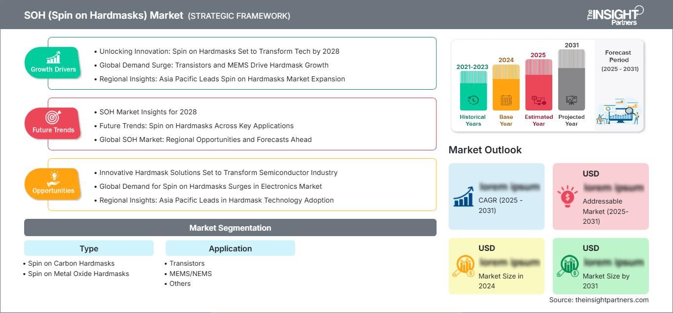
SOH (Spin on Hardmasks) Market: Strategic Insights
Regional Insights
North America SOH Market
North America represented ~18% of the SOH Market Share in 2025 and is expected to expand at a CAGR of ~8% through 2034. The regional opportunity is anchored by the US, where semiconductor manufacturing expansion is increasing demand for advanced process materials. New and expanded fabrication capacity requires qualified materials that can support lithography, etching, multilayer integration, and increasingly complex device architectures. The region also benefits from a dense ecosystem of semiconductor equipment suppliers, materials developers, chip designers, foundries, and research institutions.
Canada and Mexico are part of the bigger electronics and manufacturing environment, although higher SOH demands are centered in the United States. Requirements related to application are very significant with regards to advanced logic, memory, specialty semiconductors, and fabrication focused on research. Regional customers attach great importance to reliability in supply chain, consistent qualification, purity analysis, and sourcing resilience. This creates opportunities for those suppliers which are able to provide regional technical support and manufacturing redundancy, but still compatible with global semiconductor processing standards.
U.S. SOH Market
The United States made up roughly 88% of North American SOH Market Share in 2025 and is anticipated to register a CAGR of roughly 8% until 2034. The reason for the same is the concentration of advanced semiconductor manufacturing, development of equipment, IDM, and semiconductor research. There is encouragement from government-led fabrication investments for developing more local capabilities, thus leading to higher addressable need for specialty process materials. There is demand from logic devices, memory devices, advanced packaging, and specialty semiconductors.
There is advantage for the companies operating in the US ecosystem, which is the close location to semiconductor manufacturers and technology developers. The applications increasingly demand materials that are capable of maintaining uniformity of film, resistance to etching, and pattern fidelity in the most stringent processes. In addition, the US market becomes an experimental platform for hardmask materials that are new because there is scope for cooperation among material vendors, fabs, equipment developers, and research institutes during process development.
Europe SOH Market
The European market contributed ~15% to the global SOH market share in 2025 and is forecast to grow at a rate of ~8% through 2034. Germany is the market leader in Europe, with its strong industrial ecosystem, semiconductor ecosystem, equipment ties, and the demands of automotive electronics. France contributes to the European market via semiconductor manufacturing and research activities, whereas the UK offers strength in compound semiconductors, research, and specialized devices. Italy and Spain contribute to the European market via their demands for electronics, industrial technology, automotive systems, and semiconductor research.
Supply chain robustness, processing efficiencies, environmental management, and material qualification have become key concerns for European manufacturers. The strong industrial semiconductor ecosystem of Germany contributes to the need for premium process materials, while France’s semiconductor ecosystem creates possibilities for advanced patterning solutions. The specialized research expertise of the UK will help in evaluating and developing emerging materials. Italy offers automotive and industrial electronics market and therefore demand for semiconductor devices, whereas Spain offers growth in semiconductor research activities.
Opportunities for the region in this regard thus depend more on manufacturing with a technological component than on volume of wafers. There is also increasing incentive to invest in fab production in Europe because of policy support for semiconductor capacity there. For SOH vendors, the region offers opportunities in qualification, technical partnership, and specialty applications where reliability and environmental compliance are significant buying factors.
APAC SOH Market
APAC represented ~62% of the SOH Market in 2025 and is expected to record a CAGR of ~11% through 2034, making it the largest and fastest-growing region. China is the leading country in Asia Pacific based on the breadth of semiconductor manufacturing investment and downstream electronics demand. Japan and South Korea provide highly developed semiconductor materials and manufacturing ecosystems, while India is expanding its semiconductor infrastructure. Australia contributes through research, specialty technology, and supporting electronics capabilities.
Regional demand is strongly connected with memory, logic, foundry, and advanced packaging activity. South Korea's memory ecosystem, Japan's specialty-materials capabilities, and China's semiconductor manufacturing expansion create complementary demand conditions. India provides an emerging growth platform as fabrication and semiconductor packaging capabilities develop. Government-supported semiconductor programs, domestic supply-chain initiatives, and investment in advanced manufacturing are reinforcing regional demand for high-purity process materials.
Middle East & Africa SOH Market
The Middle East & Africa market is expected to grow at a CAGR of ~7% through 2034. Saudi Arabia and the UAE are the principal technology and investment centers in the Middle East, supported by economic diversification programs, digital infrastructure, and increasing interest in advanced electronics. South Africa contributes through its established industrial and research base, while the rest of MEA remains comparatively nascent for advanced semiconductor-material consumption.
The regional opportunity is linked to infrastructure development, electronics localization, technology investment, and the creation of advanced manufacturing capabilities. Saudi Arabia's industrial diversification agenda and the UAE's investment in digital infrastructure can support future semiconductor-related ecosystems. However, SOH demand remains closely tied to the establishment of fabrication and advanced device manufacturing rather than general electronics consumption, making regional development dependent on specialized infrastructure, technical expertise, and supply-chain formation.

Segmentation Analysis
Type
The Type segment in the SOH market divides the SOH Market into Spin on Carbon Hardmasks and Spin on Metal Oxide Hardmasks. Carbon-based systems currently provide the broader commercial base because of established integration in multilayer semiconductor patterning, while metal oxide formulations are attracting development attention for high-resolution applications. The type landscape is increasingly determined by etch selectivity, thermal stability, defect control, film uniformity, and compatibility with evolving lithography stacks.
- Spin on Carbon Hardmasks: Spin on Carbon Hardmasks are expected to grow at a CAGR of ~9% from 2026 to 2034. Their established role in multilayer pattern-transfer schemes supports recurring demand from semiconductor manufacturers. Carbon-rich materials can provide useful etch resistance and planarization characteristics, enabling thinner photoresist layers to work with underlying process stacks. Future adoption will depend on improved thermal stability, reduced shrinkage, coating uniformity, defect control, and compatibility with increasingly demanding logic and memory structures. The segment maintains broad demand where high etch resistance and multilayer pattern transfer are required. Its strategic importance comes from established qualification, process familiarity, and compatibility with complex semiconductor manufacturing flows.
- Spin on Metal Oxide Hardmasks: Spin on Metal Oxide Hardmasks are projected to expand at a CAGR of ~12% through 2034. Their growth reflects increasing interest in inorganic material systems for demanding patterning applications. Metal oxide chemistry can offer high-resolution patterning characteristics and strong resistance under selected process conditions. Adoption depends on controlling sensitivity, film uniformity, defectivity, composition, and integration with advanced lithography and etch processes. Demand is concentrated in emerging high-resolution patterning applications. The technology offers strategic value where manufacturers seek inorganic films capable of supporting increasingly precise feature definition and advanced process integration.
Application
The Application segment comprises Transistors, MEMS/NEMS, and Others. Transistor manufacturing represents the principal commercial application because advanced logic and memory devices require increasingly sophisticated pattern-transfer schemes. MEMS/NEMS provides a distinct growth avenue because microstructures can require controlled etching and durable masking. The application landscape is consequently shaped by feature geometry, substrate material, etch chemistry, production volume, and process integration requirements.
- Transistors: Transistor applications are expected to grow at a CAGR of ~10% through 2034. Advanced transistor structures require increasingly controlled patterning as manufacturers transition toward more complex architectures and smaller dimensions. SOH materials help create process stacks capable of transferring patterns through layers that cannot be adequately protected by conventional photoresists alone. Continued logic scaling, memory integration, and advanced-node manufacturing should sustain material qualification activity.
- MEMS/NEMS: MEMS/NEMS applications are expected to expand at a CAGR of ~11% through 2034. These devices use microscale and nanoscale structures that can require durable masking during deep or selective etching. SOH materials can provide process flexibility where conventional resist systems do not provide sufficient resistance or thickness control. Adoption is supported by sensors, actuators, communications components, and specialized microdevices. The application provides a specialized demand base where structural depth, material compatibility, and etch selectivity are important. Its strategic role increases as sensors and nanoscale devices require increasingly controlled fabrication processes.
Opportunity Snapshot
| Application | Revenue Contribution | Trend Tag | Adoption Stage |
| Transistors | High | Node Scaling | Mature |
| MEMS/NEMS | Medium | Deep Etching | Scaling |
| Others | Low | Specialty Devices | Emerging |
SOH (Spin on Hardmasks) Market Growth Drivers and Impact Analysis
Advanced Semiconductor Scaling Increases Pattern-Transfer Complexity
Semiconductor scaling is increasing the number of process steps and the precision required during pattern transfer, strengthening the role of hardmask materials. As device structures become more vertically integrated, conventional photoresist layers may not provide sufficient thickness or etch resistance for transferring fine patterns through underlying films. SOH materials address this requirement by creating intermediate layers that can withstand selected etch environments. The commercial impact is a shift toward formulations optimized for lower defectivity, controlled shrinkage, improved thermal performance, and stable film properties. Suppliers that demonstrate reliable performance under advanced process conditions can participate in extended qualification programs and secure recurring demand as semiconductor manufacturers move new device architectures into volume production.
Growth of Memory and High-Performance Computing Devices
Expansion of memory and high-performance computing devices is increasing the need for sophisticated semiconductor fabrication processes. Advanced DRAM, NAND, logic, and accelerator architectures require precise pattern transfer across multiple layers, making process-material performance increasingly important. AI-related computing demand also encourages semiconductor manufacturers to increase device density and performance while controlling power consumption. This creates additional requirements for materials capable of supporting tighter process windows and more complex integration. The market impact extends across both established carbon-based hardmasks and emerging inorganic systems. Suppliers able to tailor formulations to customer-specific process flows can strengthen qualification pipelines as memory and logic manufacturers expand production and introduce new process generations.
Semiconductor Supply-Chain Localization Supports Regional Material Investment
Semiconductor manufacturing localization is changing how process-material suppliers evaluate capacity, technical support, and supply continuity. Manufacturers increasingly seek geographically diversified sources for critical chemicals and process materials to reduce exposure to transportation disruptions, geopolitical restrictions, and concentrated production risks. This creates opportunities for SOH suppliers to establish regional manufacturing, purification, packaging, application laboratories, and technical-service capabilities closer to major fabrication clusters. The impact is particularly relevant in North America and emerging semiconductor locations where local production ecosystems are expanding. Localization can also shorten qualification-support cycles because suppliers can work directly with fab engineering teams. Over time, regional manufacturing footprints may become an important competitive factor alongside formulation performance and cost.
SOH (Spin on Hardmasks) Market Future Trends
Integration of Carbon and Inorganic Materials With Next-Generation Patterning
SOH Market trends increasingly point toward broader integration of carbon-based and inorganic material systems within advanced patterning stacks. Rather than relying on a single material class, semiconductor manufacturers can select different layers according to lithography wavelength, etch chemistry, thermal budget, aspect ratio, and desired critical-dimension control. This encourages suppliers to develop complementary portfolios rather than isolated formulations. Metal oxide technologies are receiving particular attention for high-resolution patterning, while carbon systems remain important for planarization and etch resistance. Future material development is therefore likely to emphasize stack-level performance, where interactions among photoresist, hardmask, etch, deposition, and cleaning steps are optimized together.
Data-Driven Materials Development Accelerates Formulation Cycles
Data-driven development is emerging as an important method for reducing the time required to identify semiconductor-material formulations. Advanced characterization generates large datasets covering composition, thermal behavior, film thickness, etch response, defectivity, and process conditions. Combining these datasets with computational chemistry and machine-learning methods can help suppliers screen candidate formulations before extensive laboratory testing. The approach can be particularly valuable for hardmask materials because performance depends on multiple interacting chemical and process variables. As semiconductor process windows become narrower, digital tools can support faster experimentation and more systematic optimization. The resulting competitive differentiation will increasingly depend on the combination of materials expertise, process data, analytical capability, and customer-specific integration knowledge.
SOH (Spin on Hardmasks) Market Opportunities
Localized Production and Application Centers Near New Fabs
SOH Market Forecasts indicate commercial opportunities for suppliers that combine manufacturing capacity with local application engineering. New semiconductor fabrication clusters require rapid material qualification, technical troubleshooting, inventory support, and analytical services. Establishing application centers near customers can shorten development cycles and allow suppliers to optimize formulations against specific coating, baking, lithography, and etch conditions. Regional production can additionally improve supply resilience where customers seek alternatives to geographically concentrated sources. Investment opportunities therefore extend beyond chemical manufacturing into purification, analytical laboratories, packaging, process simulation, and technical support. Suppliers with scalable production platforms can use regional facilities to support both established carbon formulations and emerging inorganic systems as customer requirements evolve.
Joint Development Programs for Advanced Logic and Memory Processes
A second opportunity lies in structured collaboration among hardmask suppliers, semiconductor manufacturers, lithography developers, and etch-equipment companies. Advanced patterning increasingly depends on interactions among materials and process tools, making isolated formulation development less effective for the most demanding nodes. Joint development programs can accelerate screening, process-window evaluation, defect analysis, and qualification. Suppliers can also use these relationships to develop formulations tailored to memory, logic, MEMS/NEMS, or specialty-device architectures. Commercial value can emerge from earlier participation in customer technology roadmaps, stronger technical differentiation, and longer qualification relationships. Companies with complementary expertise in organic, inorganic, deposition, and etch technologies are particularly positioned to participate in ecosystem-based development programs.
Recent Developments
- May 2026: JSR Corporation, through Inpria Corporation, announced a non-exclusive cross-licensing agreement with Entegris covering metal oxide resist patents and future photoresist collaboration. The initiative is focused on advancing EUV lithography for next-generation semiconductor manufacturing and illustrates continued development of inorganic patterning materials for advanced nodes.
- April 2026: Samsung's semiconductor ecosystem continued advancing next-generation EUV and advanced-node manufacturing, including preparations for High NA EUV and future DRAM production. The company's broader advanced-patterning roadmap supports the process environment in which high-performance hardmask and related lithography materials are qualified.
- April 2024: Shin-Etsu MicroSi — Shin-Etsu Chemical announced construction of a fourth manufacturing base for semiconductor lithography materials in Isesaki, Japan. The facility is designed to expand manufacturing and R&D capabilities and strengthen supply capacity for advanced semiconductor lithography materials, reinforcing regional production infrastructure relevant to next-generation patterning materials.
Frequently Asked Questions

- Comprehensive Market Sizing and Forecast Analysis
- Detailed Segmentation Analysis
- In-Depth Market Dynamics Assessment
- Regional and Country-Level Insights
- Competitive Landscape and Company Benchmarking
- Strategic Business Intelligence
Recent Reports
Testimonials

The Insight Partners provided valuable market intelligence that supported our global go-to-market strategy. Their team was professional, responsive, and attentive to our feedback, providing thoughtful analysis and helpful methodological clarifications throughout the project.
Junmo Kim Chief Financial Officer (CFO), Enertech Co., Ltd.
The Insight Partners' SCADA System Market report is comprehensive, with valuable insights on current trends and future forecasts. The team was highly professional, responsive, and supportive throughout. We are very satisfied and highly recommend their services.
RAN KEDEM Partner, Reali Technologies LTDs
I requested a report on a very specific software market and the team produced the report in a few days. The information was very relevant and well presented. I then requested some changes and additions to the report. The team was again very responsive and I got the final report in less than a week.
JEAN-HERVE JENN Chairman, Future Analytica
We worked with The Insight Partners for an important market study and forecast. They gave us clear insights into opportunities and risks, which helped shape our plans. Their research was easy to use and based on solid data. It helped us make smart, confident decisions. We highly recommend them.
PIYUSH NAGPAL Sr. Vice President, High Beam Global
The Insight Partners delivered insightful, well-structured market research with strong domain expertise. Their team was professional and responsive throughout. The user-friendly website made accessing industry reports seamless. We highly recommend them for reliable, high-quality research services
YUKIHIKO ADACHI CEO, Deep Blue, LLC.
This is the first time I have purchased a market report from The Insight Partners.While I was unsure at first, I visited their web site and felt more comfortable to take the risk and purchase a market report.I am completely satisfied with the quality of the report and customer service. I had several questions and comments with the initial report, but after a couple of dialogs over email with their analyst I believe I have a report that I can use as input to our strategic planning process.Thank you so much for taking the extra time and making this a positive experience.I will definitely recommend your service to others and you will be my first call when we need further market data.
JOHN SUZUKI President and Chief Executive Officer, Board Director, BK Technologies
I wish to appreciate your support and the professionalism you displayed in the course of attending to my request for information regarding to infectious disease IVD market in Nigeria. I appreciate your patience, your guidance, and the fact that you were willing to offer a discount, which eventually made it possible for us to close a deal. I look forward to engaging The Insight Partners in the future, all thanks to the impression you have created in me as a result of this first encounter.
DR CHIJIOKE ONYIA MANAGING DIRECTOR, PineCrest Healthcare Ltd.Reason to Buy
- Informed Decision-Making
- Understanding Market Dynamics
- Competitive Analysis
- Identifying Emerging Markets
- Customer Insights
- Market Forecasts
- Risk Mitigation
- Boosting Operational Efficiency
- Strategic Planning
- Investment Justification
- Tracking Industry Innovations
- Aligning with Regulatory Trends





 Get Free Sample for