
Through-silicon via (TSV) Technology Market Size, Share & Trends by 2034
Coverage: By Type (Via First TSV, Via Middle TSV, Via Last TSV); Application (Image Sensors, 3D Package, 3D Integrated Circuits, Others) , and Geography (North America, Europe, Asia Pacific, and South and Central America)
- Status : Data Released
- Report Code : TIPRE00026918
- Category : Electronics and Semiconductor
- No. of Pages : 150
- Available Report Formats :


- Last update date : July 21, 2026


2025 Market Size
US$ 4.1 Bn
Base year value
2034 Forecast
US$ 12.05 Bn
Projected by 2034
CAGR 2026-2034
14.43 %
Growth rate
Addressable Market
US$ 76.86 Bn
(2026-2034)
The Through-Silicon Via Technology Market was valued at US$ 4.1 Billion in 2025 and is projected to reach US$ 12.05 Billion by 2034, growing at a CAGR of 14.43% during 2026–2034.Demand is driven by increased density interconnects, stacked memory, image sensors, 3D packages, and 3D ICs to minimize signal distance, increase bandwidth, and create compact semiconductor designs.
North America continues to be one of the most lucrative regions, where the Through-Silicon Via Technology Market size is driven by artificial intelligence infrastructure development, advanced packaging, and fabless semiconductors. North America is projected to have a CAGR of 12.8–13.6% during 2026–2034 due to high bandwidth memory, 2.5D interposer, aerospace electronics, and compute-intensive packaging needs of the U.S.
Through-silicon via (TSV) Technology Market Assessment and Insights
- North America accounted for 28–32% share in 2025 and is growing at a CAGR range of 12.8–13.6% during 2026–2034, supported by AI servers, advanced packaging, and domestic semiconductor capacity.
- US represented 68–72% of North America in 2025 and is growing at a CAGR range of 13.0–13.8% during 2026–2034, driven by HPC and defense electronics.
- Europe held 16–19% share in 2025 and is growing at a CAGR range of 11.4–12.2% during 2026–2034, with Germany, France, the UK, Italy, and Spain leading packaging adoption.
- Asia Pacific captured 43–47% share in 2025 and is growing at a CAGR range of 15.2–16.1% during 2026–2034, led by China, Japan, South Korea, Taiwan-linked supply chains, and India.
- Largest Segment 3D Integrated Circuits held 41–45% market share in 2025, with a CAGR range of 14.6–15.4% during 2026–2034, reflecting stacked logic and memory demand.
- High Growth Segment Via Middle TSV held 30–34% market share in 2025, with a CAGR range of 15.5–16.4% during 2026–2034, due to process compatibility with advanced nodes.
- Key companies analyzed in detail: Amkor Technology, Inc.; ALLVIA, Inc.; Advanced Packaging Technology Laboratories; China Wafer Level CSP Co., Ltd.; Tianshui Huatian Technology Co., Ltd.; Intel Corporation; Micralyne Inc.; Samsung Electronics Co., Ltd.; TESCAN ORSAY HOLDING, a.s.; Xilinx, Inc.
Source: The Insight Partners' analysis based on proprietary research, government publications, company annual reports, investor presentations, industry databases, and expert interviews.
The technology trend in TSV has changed from the interconnects of image sensors to heterogeneous integration of memory, logic, MEMS, and high-performance packaging. The manufacturers are transitioning from the coarser TSV design to a fine pitch, tighter control of aspect ratio, better copper fill quality, and thermal-aware layout design. The transition will affect manufacturing trends by creating more demand for etching, deposition, metrology, bonding, and inspection equipment at foundries, OSATs, and IDMs.
During the forecast period, capital expenditure is anticipated to tilt toward Asia Pacific packaging clusters, U.S. advanced assembly capabilities, and European semiconductor sovereignty programs. Tailwind in the regulatory landscape from semiconductor sovereignty, AI ecosystem, automotive semiconductor, and supply chain security will drive the long-term demand outlook. New geographies will attract selective TSV process outsourcing based on customer demand for cost efficiencies and regional risk mitigation.
Through-silicon via (TSV) Technology Market Report Scope
| Report Attribute | Details |
|---|---|
| Market size in 2025 | US$ 4.1 Billion |
| Market Size by 2034 | US$ 12.05 Billion |
| Global CAGR (2026 - 2034) | 14.43% |
| Historical Data | 2021-2024 |
| Forecast period | 2026-2034 |
Through-silicon via (TSV) Technology Market Analysis
Demand for Through-Silicon Via Technology Market growth stems from bandwidth-heavy computing, smaller consumer electronics, and high-sensing electronic devices. TSV technology reduces signal path length and latency, making it possible to vertically stack integrated circuits where planar scaling fails to provide further gains. Artificial Intelligence servers, high-bandwidth memory, CMOS image sensors, radio frequency modules, and computer modules in automobiles are expanding the potential customer base for 2.5D and 3D packaging.
The value chain involves wafer fabrication, via etching, dielectric liner deposition, barrier and seed layering, copper plating, thinning, bonding, inspection, and final assembly. The supply side still faces challenges associated with low yield, thermal stresses, and capital intensiveness. In addition to customer demand, equipment availability and tested process recipes play an equally important role in shipments schedule and scale-up.
Competitive advantage in the Through-Silicon Via Technology Market Report is determined by process depth, packaging capability, and the customer qualification cycle. Process-oriented Amkor Technology, Inc. and Samsung Electronics Co., Ltd. focus on advanced assembly and packaging associated with memory chips, while Intel Corporation concentrates on foundry and heterogeneous integration capabilities. ALLVIA, Inc., Micralyne Inc., and TESCAN ORSAY HOLDING, a.s. offer expertise in via etching, MEMS, and inspection.
The investment trends point towards those businesses which have the capability to leverage their knowledge of TSV along with wafer level packaging, design enablement, and reliability testing. China Wafer Level CSP Co., Ltd. and Tianshui Huatian Technology Co., Ltd. provide greater choice for Asia-focused outsourced business, while Xilinx, Inc. gains importance due to its high performance programmable logic ecosystem.
● REPORT CUSTOMIZATION
Tailor This Report To Align With Your Specific Business Requirements
This report can be customized to align precisely with your business objectives, scope, and target markets. Customization options include tailored segmentation, geography, competitive analysis, and strategic insights to support informed decision-making.
Customize This Report →WHAT YOU CAN ADJUST
- ● Segmentations
- ● Geography
- ● Competitive Analysis
- ● Language Preferences
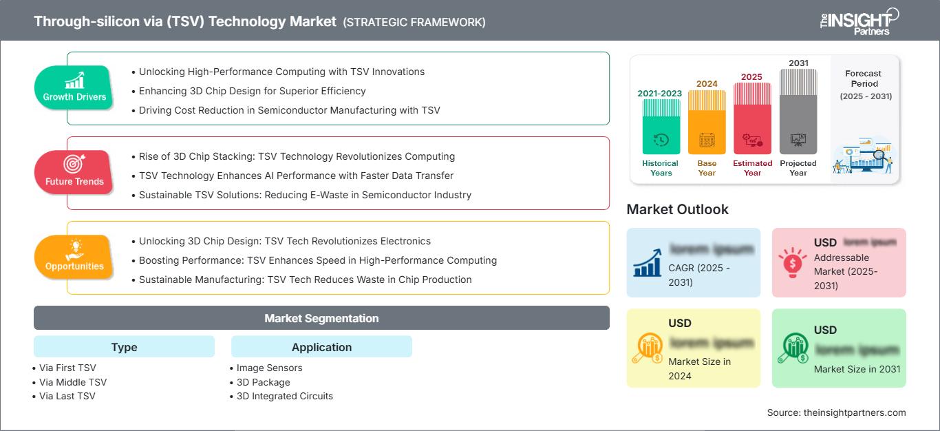
Through-silicon via (TSV) Technology Market: Strategic Insights
Regional Insights
North America Through-Silicon Via Technology Market
North America held 28–32% Through-Silicon Via Technology Market share in 2025 and is forecast to expand at a 12.8–13.6% CAGR during 2026–2034. The region benefits from AI accelerator demand, advanced packaging roadmaps, defense-grade electronics, and strong design activity. U.S. semiconductor policy and domestic packaging programs are improving the business case for local TSV process qualification.
Growth is strongest where high-bandwidth memory, interposers, and stacked logic are linked to data center platforms. Customers prioritize secure supply, known-good-die availability, and shorter qualification loops. The regional ecosystem also benefits from materials suppliers, metrology companies, and OSAT investments that support via etch, copper fill, wafer thinning, and reliability validation.
U.S. Through-Silicon Via Technology Market
The U.S. represented 68–72% of North America in 2025 and is expected to grow at a 13.0–13.8% CAGR during 2026–2034. Demand centers around AI servers, aerospace electronics, FPGA platforms, CMOS imagers, and secure computing. Domestic relevance is promoted by Intel Corporation and Xilinx, Inc. through high-end compute architecture and programmable logic.
Applications reveal an increasing trend towards the adoption of TSV technology in 3D ICs and 3D packages where the bandwidth limit at the package level poses a constraint. Reliability, thermal performance, and traceability are among the key criteria considered by U.S. buyers of these components. This leaves space for the emergence of advanced packaging service providers, equipment companies, and process experts.
Europe Through-Silicon Via Technology Market
Europe accounted for 16–19% share in 2025 and is projected to grow at an 11.4–12.2% CAGR during 2026–2034. Germany is the leading country thanks to automotive electronics, industrial automation, and sensors. The contribution from the UK includes compound semiconductors and design capabilities, while France is contributing in aerospace, defense, and imaging.
The countries such as Italy and Spain contribute in demand generation because of industrial electronics, medical devices, and microelectronics efforts aimed at resilience in the region. Programs in Europe stimulate advanced packaging capability; however, scale is lagging behind Asia Pacific and North America. Suppliers who can provide automotive reliability, low-defect, and longer lifecycle products will have an advantage.
APAC Through-Silicon Via Technology Market
Asia Pacific held 43–47% share in 2025 and is forecast to grow at a 15.2–16.1% CAGR during 2026–2034, making it the leading regional market. China, Japan, South Korea, India, and Australia support demand through memory, image sensors, display electronics, and advanced packaging investment.
South Korea leads in memory-linked TSV adoption, while China expands wafer-level packaging and outsourced assembly. Japan contributes materials, equipment, and precision manufacturing, and India is building semiconductor policy momentum. Industrial capacity, customer proximity, and government-backed semiconductor programs reinforce the region’s long-term advantage.
Middle East & Africa Through-Silicon Via Technology Market
Middle East & Africa is expected to expand at a 9.2–10.0% CAGR during 2026–2034, with Saudi Arabia and the UAE leading demand from data centers, energy infrastructure, and industrial digitalization. South Africa adds electronics assembly and research activity, while the rest of MEA remains import dependent.
Regional adoption is early but improving as sovereign cloud, AI infrastructure, and smart-city programs increase requirements for advanced chips. TSV demand is largely indirect through imported servers, sensors, and communications hardware. Local opportunity depends on electronics assembly depth, semiconductor partnerships, and long-term infrastructure procurement.
Segmentation Analysis
Type
Type segment in the Through-Silicon Via Technology Market is projected to grow at a 14.0–14.8% CAGR during 2026–2034 as process selection becomes central to yield, cost, and device compatibility. The Through-Silicon Via Technology Market scope across via first, via middle, and via last approaches reflects different integration points in wafer fabrication and packaging flows.
- Via First TSV remains important for early integration schemes where vias are created before front-end device completion, supporting compact designs but requiring tight process control and strong thermal compatibility.
- Via Middle TSV is strategically important in advanced logic and memory flows because it balances wafer-level integration flexibility with better alignment to semiconductor process windows.
- Via Last TSV supports packaging-stage integration, especially where manufacturers seek lower front-end disruption, broader outsourcing flexibility, and compatibility with mature wafer processing environments.
Application
Application segment in the Through-Silicon Via Technology Market is expected to grow at a 14.5–15.3% CAGR during 2026–2034 as TSV adoption expands from imaging into stacked computing and high-density packaging. Device makers select TSV-based architectures when signal distance, form factor, power efficiency, and bandwidth requirements cannot be addressed through conventional interconnects.
- Image Sensors continue to use TSVs for compact camera modules, mobile imaging, automotive cameras, medical imaging, and wafer-level packaging where lower profile and reliable electrical routing are essential.
- 3D Package demand is rising as chiplet, interposer, and stacked package designs address bandwidth and space limits in AI, networking, consumer electronics, and automotive platforms.
- 3D Integrated Circuits represent the largest application base because vertical die stacking improves integration density, reduces interconnect length, and supports high-performance memory and logic combinations.
Opportunity Snapshot
| Application | Revenue Contribution | Trend Tag | Adoption Stage |
| Image Sensors | Medium | Compact Imaging | Mature |
| 3D Package | High | Chiplet Stack | Scaling |
| 3D Integrated Circuits | High | HBM Logic | Scaling |
Through-silicon via (TSV) Technology Market Growth Drivers and Impact Analysis
AI and High-Bandwidth Memory Demand
The workload of memory bandwidth required for training and inference of AI cannot be delivered effectively by the current architecture on boards. The high bandwidth memory stack made possible through TSV reduces interconnect lengths, consumes lower energy per bit transfer, and increases the density of packages for the accelerators and data center processors. This creates an increased demand for via etch, copper fill, wafer thinning, and bonding capabilities. The effect is most profound in the advanced packaging lines that are used for AI accelerators.
Miniaturization Across Imaging and Edge Devices
Smartphones, automobile cameras, medical devices, wearable devices, and industrial sensors are among the applications that need ever-smaller and more functional modules. TSV technology permits image sensors and other stacked devices to reroute their electrical connections to a vertical path rather than occupying valuable real estate on the device, thus allowing the package to become thinner. The practical effects of this can be seen in greater numbers of design wins by wafer-level packaging companies, as well as differentiation for camera and sensor modules.
Semiconductor Sovereignty and Packaging Investment
Governments and manufacturers are treating advanced packaging as a strategic capability rather than a back-end service. Policy support in the U.S., Europe, Japan, South Korea, China, and India is encouraging investment in assembly, test, substrates, and packaging process development. TSV capacity benefits because it is critical to 2.5D and 3D integration. The market impact is a wider pool of qualified facilities, stronger regional supply security, and greater customer willingness to fund co-development for mission-critical applications.
Through-silicon via (TSV) Technology Market Future Trends
Thermal-Aware TSV Design
Future Through-Silicon Via Technology Market trends will increasingly focus on thermal-aware design rules that integrate via placement, keep-out zones, materials, and package-level heat paths from the earliest architecture stage. As 3D stacks grow taller, thermal stress and localized heating can limit reliability before electrical performance reaches its ceiling. Suppliers that combine simulation, metrology, and process control will help customers reduce requalification risk. This trend will shift TSV decisions from a manufacturing-only discussion to a system-level co-optimization requirement.
Finer Pitch and Hybrid Integration
Future packaging technology needs fine-pitch TSV technology, better overlay control, and greater compatibility with hybrid bonding and RDL processes. The objective is to facilitate chiplets, memory stacks, RF functionality, and sensors in packages that offer higher bandwidth per square millimeter. This transition will benefit those with superior capabilities in lithography, etch process uniformity, copper plating process management, and inspection. Eventually, fine-pitch TSV technology will be the enabler layer for heterogeneous semiconductor platforms, not just another interconnect option.
Through-silicon via (TSV) Technology Market Opportunities
Advanced Packaging Partnerships for AI Infrastructure
Through-Silicon Via Technology Market Forecasts indicate strong opportunity for packaging partnerships serving AI accelerators, high-bandwidth memory, and networking silicon. Foundries, OSATs, memory suppliers, and equipment vendors can create joint process roadmaps that reduce customer qualification time. Investors should prioritize platforms with proven reliability testing, thermal modeling, and scalable wafer-level capacity. The best opportunities will arise where suppliers can guarantee yield learning, secure capacity, and co-design support for hyperscale and enterprise computing customers.
Regional Outsourcing for Cost and Supply Resilience
There is a real possibility for the customers of semiconductors to achieve cost management and diversification through regional outsourcing. While Asia Pacific will continue to dominate as the largest producer, North American and European customers will have their secondary TSV lines and advanced packaging qualify for resilience. There is differentiation possible on service through process transparency, automotive-grade quality, and flexible capacity model. The possibility is particularly interesting for mid-volume applications where one wants to harness advanced packaging capability without making any capital investment in manufacturing.
Recent Developments
- June 2026: Amkor Technology, Inc. — the company highlighted next-generation packaging and U.S. expansion activity at ECTC 2026, reinforcing its positioning in advanced assembly for AI, high-performance computing, and heterogeneous integration applications that can use TSV-enabled architectures.
- May 2026: Samsung Electronics Co., Ltd. — Samsung began shipment of industry-first HBM4E samples, advancing high-bandwidth memory roadmaps that rely on stacked memory architectures and TSV interconnects for AI computing platforms.
- June 2026: Intel Corporation — Intel Foundry detailed process milestones and future innovation at the VLSI Symposium, supporting its broader advanced manufacturing and packaging strategy for next-generation compute platforms.
Frequently Asked Questions

- Comprehensive Market Sizing and Forecast Analysis
- Detailed Segmentation Analysis
- In-Depth Market Dynamics Assessment
- Regional and Country-Level Insights
- Competitive Landscape and Company Benchmarking
- Strategic Business Intelligence
Recent Reports
Testimonials

The Insight Partners' SCADA System Market report is comprehensive, with valuable insights on current trends and future forecasts. The team was highly professional, responsive, and supportive throughout. We are very satisfied and highly recommend their services.
RAN KEDEM Partner, Reali Technologies LTDs
I requested a report on a very specific software market and the team produced the report in a few days. The information was very relevant and well presented. I then requested some changes and additions to the report. The team was again very responsive and I got the final report in less than a week.
JEAN-HERVE JENN Chairman, Future Analytica
We worked with The Insight Partners for an important market study and forecast. They gave us clear insights into opportunities and risks, which helped shape our plans. Their research was easy to use and based on solid data. It helped us make smart, confident decisions. We highly recommend them.
PIYUSH NAGPAL Sr. Vice President, High Beam Global
The Insight Partners delivered insightful, well-structured market research with strong domain expertise. Their team was professional and responsive throughout. The user-friendly website made accessing industry reports seamless. We highly recommend them for reliable, high-quality research services
YUKIHIKO ADACHI CEO, Deep Blue, LLC.
This is the first time I have purchased a market report from The Insight Partners.While I was unsure at first, I visited their web site and felt more comfortable to take the risk and purchase a market report.I am completely satisfied with the quality of the report and customer service. I had several questions and comments with the initial report, but after a couple of dialogs over email with their analyst I believe I have a report that I can use as input to our strategic planning process.Thank you so much for taking the extra time and making this a positive experience.I will definitely recommend your service to others and you will be my first call when we need further market data.
JOHN SUZUKI President and Chief Executive Officer, Board Director, BK Technologies
I wish to appreciate your support and the professionalism you displayed in the course of attending to my request for information regarding to infectious disease IVD market in Nigeria. I appreciate your patience, your guidance, and the fact that you were willing to offer a discount, which eventually made it possible for us to close a deal. I look forward to engaging The Insight Partners in the future, all thanks to the impression you have created in me as a result of this first encounter.
DR CHIJIOKE ONYIA MANAGING DIRECTOR, PineCrest Healthcare Ltd.Reason to Buy
- Informed Decision-Making
- Understanding Market Dynamics
- Competitive Analysis
- Identifying Emerging Markets
- Customer Insights
- Market Forecasts
- Risk Mitigation
- Boosting Operational Efficiency
- Strategic Planning
- Investment Justification
- Tracking Industry Innovations
- Aligning with Regulatory Trends





 Get Free Sample for