
Film Thickness Measurement Market Size, Share & Trends by 2034
Coverage: by Film Type (Dry Film, Wet Film); Technology (Eddy Current, Magnetic Induction, Optical, Ultrasonic); Application (Aerospace and Aviation, Automotive, Food and Pharmaceutical Packaging, Industrial and Manufacturing, Medical, Semiconductors, Others) , and Geography (North America, Europe, Asia Pacific, and South and Central America)
- Status : Data Released
- Report Code : TIPRE00011489
- Category : Electronics and Semiconductor
- No. of Pages : 150
- Available Report Formats :


- Last update date : September 09, 2026


2025 Market Size
US$ 1.26 Bn
Base year value
2034 Forecast
US$ 2.63 Bn
Projected by 2034
CAGR 2026-2034
8.52 %
Growth rate
Addressable Market
US$ 17.45 Bn
(2026-2034)
Film Thickness Measurement Market is positioned at the intersection of precision metrology, advanced manufacturing, and quality assurance. The size of the market stands at US$ 1.26 Billion in 2025 and is estimated to grow to reach US$ 2.63 Billion by 2034, growing at a CAGR of 8.52% during 2026–2034. The demand drivers include the increased stringency of coating tolerances, semiconductor process intricacy, automation in inspection, and increasing use of non-contact measurement in high value manufacturing.
Adoption in North America is predicted to be steady and is estimated to grow with a CAGR of 7.00-7.50% during 2026-2034. The factors behind the growth include investments in semiconductor manufacturing facilities, aerospace manufacturing, medical devices, and coating processes of vehicles. Process automation and localization of electronic manufacturing drives the demand for measurement solutions which offer repeatable and traceable thickness information without disturbing manufacturing operations.
Film Thickness Measurement Market Assessment and Insights
- North America: North America is expected to retain a substantial position, with a 2025 share of 27–31% and a CAGR of 7.00–7.50% between 2026–2034, supported by semiconductor, aerospace, medical, and automotive manufacturing.
- US: The US represents 68–72% of North American demand in 2025 and is expected to grow at a 7.20–7.70% CAGR during 2026–2034, led by semiconductor and aerospace applications.
- Europe: Europe is projected to hold a 24–28% share in 2025 and grow at 8.00–8.50% during 2026–2034, with Germany, France, the UK, Italy, and Spain supporting demand through automotive, industrial, and semiconductor activity.
- Asia Pacific: Asia Pacific is estimated at 30–34% share in 2025 and is expected to expand at 9.50–10.00%, led by China, Japan, South Korea, India, and Taiwan through electronics, semiconductor, automotive, and packaging manufacturing.
- Largest Segment: Industrial and Manufacturing is estimated to hold a 25–29% market share in 2025 and grow at 7.20–7.70% during 2026–2034, reflecting broad coating-control requirements.
- High Growth Segment: Semiconductors represent an estimated 16–20% share in 2025 and are projected to expand at 10.50–11.20% during 2026–2034, driven by advanced process control.
- Key companies analyzed in detail: ALTANA group (BYK-Gardner), Bruker, DEFELSKO CORPORATION, Elcometer Limited, ElektroPhysik, Fischer Technology Inc., Hamamatsu Photonics K.K., Horiba, Ltd., KEYENCE CORPORATION, KLA Corporation.
Source: The Insight Partners' analysis based on proprietary research, government publications, company annual reports, investor presentations, industry databases, and expert interviews.
Film Thickness Measurement Market has gone from a reliance on largely manual coating inspections to automated non-contact, digital-enabled metrology systems. Reflectometry, ellipsometry, interferometry, eddy current technology, magnetic induction and ultrasonic methods cater to varying substrate and film combinations. Production trends have pushed more towards repeatable, rapid sampling, automated mapping and assisted analysis. The semiconductor industry has especially contributed to a transition to precise multi-layer measurement, while manufacturers in the auto, aerospace, medical, and packaging sectors have been modernizing their inspection capabilities.
The future forecast looks towards Asia-Pacific manufacturing growth, semiconductor localization, advanced packaging, and functional coatings. North American investments in domestic chip production and European industrial advancements will help continue capital investments in process control equipment. Regulations that require product consistency, traceability, coating performance, and material efficiency are also driving manufacturers to move away from sporadic inspections to metrological processes that produce data.
Film Thickness Measurement Market Report Scope
| Report Attribute | Details |
|---|---|
| Market size in 2025 | US$ 1.26 Billion |
| Market Size by 2034 | US$ 2.63 Billion |
| Global CAGR (2026 - 2034) | 8.52% |
| Historical Data | 2021-2024 |
| Forecast period | 2026-2034 |
Film Thickness Measurement Market Analysis
Film Thickness Measurement Market requirements are becoming more aligned with the yield within the manufacturing process than after inspection. Semiconductors need film thickness management for dielectric, conductor, barrier, and multilayer materials. Automotive and aerospace need film thickness measurement for managing their corrosion resistance, aesthetics, and functionality. Packaging needs uniform barrier films and medical devices need film thickness management. This broad usage will ensure demand diversification.
The value chain includes component suppliers, instrument suppliers, software suppliers, calibration suppliers, integrators, and industrial users. There are changes in supply dynamics towards modular systems which allow the control of various materials and measurement range. Inline systems have gained relevance due to the ability to detect process drift earlier, avoid reworks, and link measurement results to manufacturing controls systems. In such a way, equipment suppliers offer more services, including accuracy, throughput, integration, applications, and lifecycle support.
The competitive position of the companies highlighted in the Film Thickness Measurement Market Report is based on unique coating inspection technology and semiconductor metrology. The ALTANA group (BYK-Gardner) provides many devices for coatings and industrial applications; Bruker concentrates on spectroscopic ellipsometry and reflectometry for demanding thin-film applications. KLA Corporation is positioned well in semiconductor process control that includes film thickness metrology, and KEYENCE CORPORATION competes through industrial automation and optical measuring devices. It gives opportunities to differentiate the products by means of the measurement architecture.
Increasingly, investments go to automation, high-throughput sensors, interconnectivity and application-specific design. Hamamatsu Photonics K.K. improves its solutions in high-speed wafer measuring technology; Fischer Technology Inc., ElektroPhysik, DEFELSKO CORPORATION and Elcometer Limited supply industrial coating inspection equipment. Horiba, Ltd. and others precision instrument providers offer new ways of measurements in materials development and manufacturing processes. The competitive advantages in this industry are achieved via application experience, services for installed base, calibration, integration into customer quality system.
● REPORT CUSTOMIZATION
Tailor This Report To Align With Your Specific Business Requirements
This report can be customized to align precisely with your business objectives, scope, and target markets. Customization options include tailored segmentation, geography, competitive analysis, and strategic insights to support informed decision-making.
Customize This Report →WHAT YOU CAN ADJUST
- ● Segmentations
- ● Geography
- ● Competitive Analysis
- ● Language Preferences
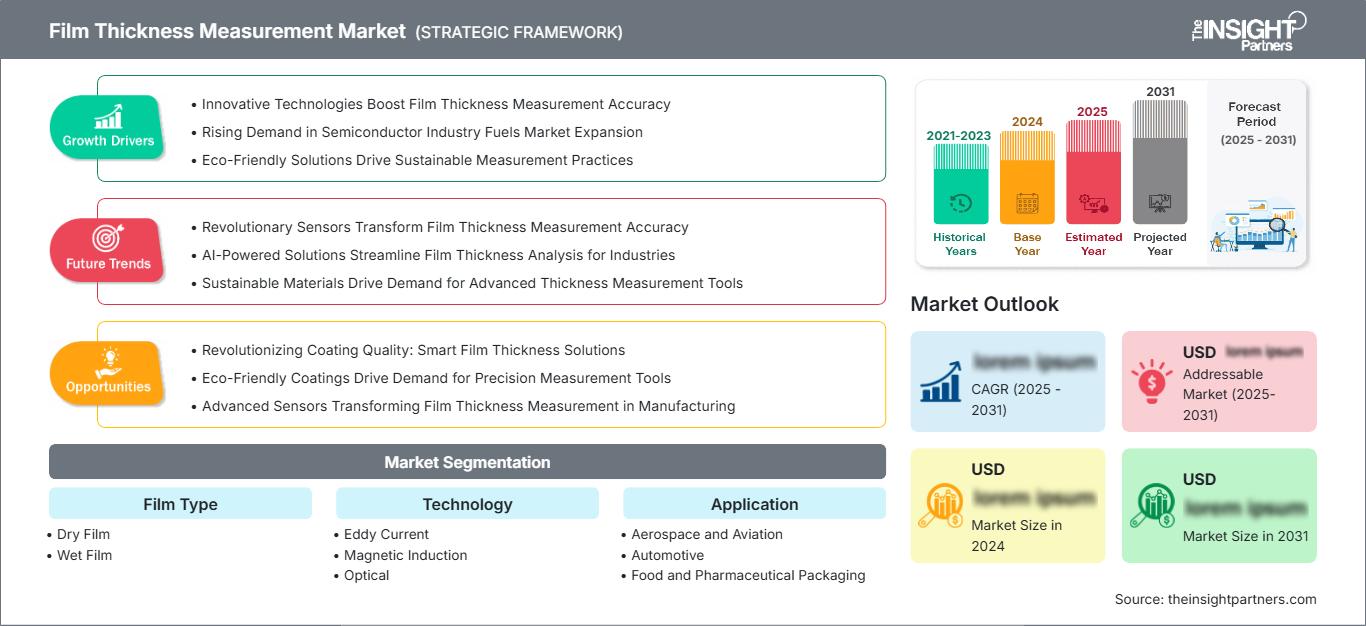
Film Thickness Measurement Market: Strategic Insights
Regional Insights
North America Film Thickness Measurement Market
The North American region is estimated to account for 27–31% of Film Thickness Measurement Market Share in 2025 and to experience a growth rate of 7.00–7.50% up to 2034. In the region, the United States accounts for 68–72% of total demand. Expansion in semiconductor fabrication facilities, aerospace manufacture, medical device manufacture, and industrial surface coatings offer a range of customers for precision measurement devices.
The strength of the region lies in its level of automation and quality control. Involvement of semiconductor manufacture leads to higher need for non-contact wafer metrology, while aerospace and defense manufacture stresses proven performance of the coating. Automotive manufacture also needs repeatability for measurements of painted, plated, and functional surfaces. Canada is involved in aerospace, mining equipment, and industrial manufacture.
U.S. Film Thickness Measurement Market
The US is contributing 68-72% of North American demand in 2025 and forecasted to increase by 7.20-7.70% until 2034. Process control investments in semiconductors are an important catalyst and supplemented by aerospace, automotive, packaging, and medical devices production. Some of the companies supplying technology and services to the local market include KLA Corporation, Bruker, KEYENCE CORPORATION, Fischer Technology Inc., and others.
There is an increasing trend towards the adoption of automatic and traceable inspection systems. While the semiconductor industry needs an inspection solution that can inspect several layers at once, the aerospace and automotive sectors are focused on having consistent coatings and corrosion resistance. The medical and packaging industries require traceable quality control because of regulations.
Europe Film Thickness Measurement Market
Europe will have a market share ranging between 24 and 28 percent in 2025 and is expected to increase by 8.00 – 8.50 percent over 2034. Germany leads in Europe due to automotive production, machinery, coatings, and semiconductor manufacturing. Other countries in Europe such as UK, France, Italy, and Spain create further demand through aerospace, automotive, packaging, medical and industrial manufacturing.
The UK will continue creating demand for coatings in aerospace, defense, advanced materials, and automotive manufacturing where consistent coatings contribute to performance. Germany has the widest industrial base which is further bolstered by automotive manufacturing, precision manufacturing, coatings, and semiconductor manufacturing. France contributes through aerospace and industrial manufacturing while Italy and Spain provide automotive components, packaging, machinery, and coatings. Increasingly, European manufacturers prefer automated traceable measurement.
APAC Film Thickness Measurement Market
APAC has an estimated 30–34% market share in 2025 and is expected to grow at 9.50–10.00%, becoming the fastest-growing region. The main driver of demand is China, then Japan, South Korea, India, and Australia. The factors driving demand include semiconductor capacity expansion, electronics manufacturing, automotive production, and packaging production.
Demand drivers are being supported by the industrial policies of localization of semiconductors, advanced manufacturing, and electronics manufacturing. The main drivers for Japan and South Korea are precise electronics and semiconductor manufacturing, India is developing its electronics manufacturing capabilities, while China combines large scale electronics manufacturing and automotive manufacturing, battery manufacturing, and industrial manufacturing.
Middle East & Africa Film Thickness Measurement Market
MEA is anticipated to have a compound annual growth rate of 6.00–6.50% between 2026 and 2034. Saudi Arabia will drive demand within the region, followed by UAE and South Africa. Diversification of industry, infrastructural developments, energy projects, automotive parts, and protective coatings will drive demand for portable and automated systems for thickness testing.
Saudi Arabia and UAE are building infrastructure outside their oil industries that will create a need for coatings' quality assessment. South Africa will drive the demand due to mining activities, industrial equipment, auto manufacturing, and infrastructural developments. The remainder of MEA is fragmented, with most of the demand driven by energy, construction, transportation, and industrial development projects.
Segmentation Analysis
Film Type
Film Type segment in the Film Thickness Measurement Market is expected to expand at a 7.80–8.30% CAGR during 2026–2034. Dry and wet coatings require different inspection approaches because substrate condition, curing state, conductivity, transparency, and surface geometry influence measurement selection. Demand is therefore shaped by the need for reliable measurements across production stages rather than by a single universal technology.
- Dry Film: Dry-film inspection remains important for cured paints, protective coatings, plating, and finished industrial components, supporting quality verification after curing and enabling documented conformity with specified coating thickness.
- Wet Film: Wet-film measurement supports process adjustment before curing, helping coating operators control application thickness, material consumption, and final performance while reducing the risk of costly downstream correction.
Technology
Technology segment in the Film Thickness Measurement Market is projected to grow at an 8.60–9.10% CAGR through 2034. Selection depends on substrate conductivity, film composition, transparency, thickness, surface condition, required accuracy, and whether contact with the measured surface is acceptable. Optical methods increasingly benefit from automation, while established electromagnetic and ultrasonic techniques remain important for industrial coatings.
- Eddy Current: Eddy-current systems are suited to non-ferrous conductive substrates and coatings, offering rapid measurements that support automotive, industrial, and quality-control workflows where portable inspection is valuable.
- Magnetic Induction: Magnetic-induction systems remain widely relevant for non-destructive coating measurement on ferrous substrates, particularly where rugged handheld instruments and straightforward field operation are priorities.
- Optical: Optical measurement is strategically important for thin and multilayer films because it enables non-contact characterization and supports advanced semiconductor, photonics, display, and precision-coating applications.
- Ultrasonic: Ultrasonic methods provide measurement flexibility for thicker coatings and multilayer structures, supporting applications where electromagnetic or optical approaches are constrained by substrate or material characteristics.
Application
Application segment in the Film Thickness Measurement Market is forecast to grow at an 8.90–9.40% CAGR during 2026–2034. Semiconductor manufacturing represents the fastest-growing application because increasingly complex film stacks require high precision and process feedback. Industrial and manufacturing uses remain the largest demand base because coating thickness influences corrosion protection, durability, appearance, and material efficiency across numerous production environments.
- Aerospace and Aviation: High-value aircraft components require controlled protective and functional coatings, making repeatable thickness measurement important for corrosion resistance, thermal management, durability, and documented manufacturing quality.
- Automotive: Automotive production uses thickness inspection across paints, primers, plating, and functional coatings, with demand strengthened by automation, electric-vehicle components, lightweight materials, and increasingly complex electronic systems.
- Food and Pharmaceutical Packaging: Packaging manufacturers depend on controlled coating and multilayer-film thickness to support barrier performance, material efficiency, seal integrity, and consistent product protection across high-volume production.
- Industrial and Manufacturing: Industrial applications form the broadest demand base because coatings are used for corrosion protection, wear resistance, decoration, insulation, and process functionality across machinery, fabricated components, and engineered products.
- Medical: Medical applications require controlled coatings on devices and components where thickness can affect functionality, durability, surface characteristics, and manufacturing consistency under demanding quality-management requirements.
- Semiconductors: Semiconductor manufacturing requires advanced measurement for multilayer dielectric, metal, barrier, and functional films, with automation and high-throughput process control becoming increasingly important as device structures become more complex.
Opportunity Snapshot
| Application | Revenue Contribution (High/Medium/Low) | Trend Tag | Adoption Stage |
|---|---|---|---|
| Aerospace and Aviation | Medium | Coating Control | Mature |
| Automotive | High | EV Coatings | Scaling |
| Food and Pharmaceutical Packaging | High | Barrier Films | Scaling |
| Industrial and Manufacturing | High | Process Control | Mature |
| Medical | Medium | Device Coatings | Scaling |
| Semiconductors | High | Wafer Metrology | Scaling |
Film Thickness Measurement Market Growth Drivers and Impact Analysis
Advanced semiconductor architectures increase metrology intensity
Semiconductor wafer fabrication is driving growth and complexity in film control needs for deposition, etching, patterning, and packaging. Characterization of dielectric, conductive, barrier, and optical films is critical for advanced logic, memory, compound semiconductor, and heterogeneous integration processes. There is a need for metrology solutions that enable interface discrimination without wafer damage and production stoppage. The business opportunity goes beyond instrument sales since fabs need more automation, recipe management, data connectivity, and service. Metrology suppliers who combine thickness measurement with refractive index, composition, stress, or topography can solve more process control needs with fewer separate systems. Measurement performance now correlates with process stability and equipment utilization.
Automation converts measurement from inspection into process control
Increasingly, manufacturers are including measurement systems within the production process rather than relying on laboratory measurements or end-of-line testing. In-line sampling makes it possible to spot deviations from standards at or near the source, lowering scrap rates and decreasing the time required for any correction processes. In-line measurement is especially useful for continuous coating applications, high speed packaging operations, semiconductor wafer production and automotive manufacturing. Some examples of market effects include increased demand for smaller sensors, robotics, in-line measurement mapping, standard interfaces and software to translate data into action. This also means that equipment vendors can add value to the process through integration and services rather than just instruments. The trend plays to the strengths of those vendors who already have well-established calibration procedures and applications databases because customers need to achieve repeatability at multiple sites.
Functional coatings broaden measurement requirements across industries
Coatings are increasingly designed to provide specific properties rather than merely improve appearance or corrosion resistance. Thermal barriers, wear-resistant layers, optical coatings, conductive films, antimicrobial surfaces, and advanced packaging barriers require controlled thickness because performance can change materially with layer variation. This expands the addressable customer base beyond conventional paint and plating inspection. Aerospace, medical, energy, automotive electronics, and industrial equipment manufacturers increasingly need measurement methods compatible with complex substrates and specialized materials. The commercial effect is a wider mix of instrument configurations, including portable gauges for field inspection, benchtop systems for laboratory verification, and automated platforms for production. Suppliers that can support multiple measurement principles and provide application-specific calibration are better positioned to serve these diversified requirements.
Film Thickness Measurement Market Future Trends
AI-assisted interpretation and autonomous measurement workflows
Film Thickness Measurement Market trends are moving toward intelligent systems that combine measurement, material models, process history, and automated decision rules. Future platforms are likely to use machine-learning techniques to identify abnormal thickness distributions, distinguish measurement artifacts from genuine process drift, and recommend sampling adjustments. Semiconductor fabs could connect film data with broader process-control datasets, while coating manufacturers could use automated alerts to correct application parameters before material reaches downstream stages. Hardware development is also expected to emphasize smaller footprints, robotic handling, wider measurement envelopes, and faster mapping. The result will be a gradual shift from instruments that simply report thickness toward systems that interpret measurement context and support autonomous production decisions.
Multimodal metrology for complex multilayer structures
Future systems are likely to combine optical, electromagnetic, ultrasonic, and surface-characterization capabilities to address increasingly diverse materials. A single production environment may contain metallic coatings, polymers, ceramics, transparent films, and multilayer stacks that cannot be measured reliably through one principle alone. Multimodal architectures can reduce instrument switching, simplify process qualification, and provide complementary information about thickness, uniformity, refractive behavior, or surface condition. Demand should be strongest in semiconductor, advanced packaging, photonics, and specialty industrial applications where material combinations are changing rapidly. Suppliers will increasingly differentiate through software that selects suitable measurement models automatically and reconciles outputs from different sensing modes. This could improve utilization while lowering operator dependence.
Film Thickness Measurement Market Opportunities
Regional semiconductor ecosystems create equipment localization opportunities
Film Thickness Measurement Market Forecasts indicate attractive opportunities for suppliers that localize engineering, calibration, service, and application development around emerging semiconductor manufacturing clusters. Asia Pacific offers the broadest opportunity because China, Japan, South Korea, Taiwan, and India are strengthening electronics and semiconductor capabilities. North America and Europe also provide opportunities as domestic production initiatives encourage new fabs and advanced packaging capacity. Suppliers can improve market access by establishing application laboratories near customers, qualifying measurement recipes with local materials, and maintaining spare-parts inventories within major manufacturing regions. Partnerships with equipment integrators can further reduce implementation barriers. The most defensible opportunity lies in combining localized technical support with globally consistent measurement standards, enabling customers to transfer validated processes across production facilities.
Integrated coating analytics can unlock higher-value industrial accounts
Industrial manufacturers increasingly need more than a single thickness reading. An opportunity exists to combine coating thickness with surface roughness, gloss, color, adhesion, curing information, or environmental conditions within a unified quality workflow. Such systems could help automotive, aerospace, medical, and industrial producers correlate coating parameters with finished-product performance. Vendors can pursue this opportunity through modular software, connected handheld devices, automated inspection cells, and subscription-based data services. Integration with manufacturing execution and statistical process-control systems can also create recurring value after the initial equipment purchase. The commercial strategy should focus on measurable reductions in rework, material consumption, inspection time, and warranty exposure rather than simply emphasizing instrument accuracy. This approach can support broader adoption among large multi-site manufacturers.
Recent Developments
- December 2025: Rigaku launched the XTRAIA MF-3400, a next-generation thin-film metrology system designed for high-precision, nondestructive measurement of semiconductor films. The system combines X-ray reflectivity, X-ray fluorescence and X-ray diffraction to measure film thickness, density, composition and crystallinity, delivering sub-nanometer thickness measurement on fields as narrow as 50 µm. With up to twice the measurement capacity of its predecessor and adoption planned by KIOXIA for 3D NAND mass-production lines, the system supports growing demand for high-throughput and nanoscale film thickness measurement in advanced semiconductor manufacturing.
- April 2025: Inteplast Group upgraded thickness measurement systems on two BOPP film production lines in Texas by replacing radioactive-source gauges with infrared-based NDC thickness scanners supplied through Brückner Servtec. The retrofit, combined with Brückner’s thickness control software, is designed to provide more precise and reliable film thickness measurements while improving workplace safety and production quality. The upgrade highlights the shift toward non-radioactive, automated thickness measurement technologies in plastic film manufacturing.
Frequently Asked Questions

- Comprehensive Market Sizing and Forecast Analysis
- Detailed Segmentation Analysis
- In-Depth Market Dynamics Assessment
- Regional and Country-Level Insights
- Competitive Landscape and Company Benchmarking
- Strategic Business Intelligence
Recent Reports
Testimonials

The Insight Partners' SCADA System Market report is comprehensive, with valuable insights on current trends and future forecasts. The team was highly professional, responsive, and supportive throughout. We are very satisfied and highly recommend their services.
RAN KEDEM Partner, Reali Technologies LTDs
I requested a report on a very specific software market and the team produced the report in a few days. The information was very relevant and well presented. I then requested some changes and additions to the report. The team was again very responsive and I got the final report in less than a week.
JEAN-HERVE JENN Chairman, Future Analytica
We worked with The Insight Partners for an important market study and forecast. They gave us clear insights into opportunities and risks, which helped shape our plans. Their research was easy to use and based on solid data. It helped us make smart, confident decisions. We highly recommend them.
PIYUSH NAGPAL Sr. Vice President, High Beam Global
The Insight Partners delivered insightful, well-structured market research with strong domain expertise. Their team was professional and responsive throughout. The user-friendly website made accessing industry reports seamless. We highly recommend them for reliable, high-quality research services
YUKIHIKO ADACHI CEO, Deep Blue, LLC.
This is the first time I have purchased a market report from The Insight Partners.While I was unsure at first, I visited their web site and felt more comfortable to take the risk and purchase a market report.I am completely satisfied with the quality of the report and customer service. I had several questions and comments with the initial report, but after a couple of dialogs over email with their analyst I believe I have a report that I can use as input to our strategic planning process.Thank you so much for taking the extra time and making this a positive experience.I will definitely recommend your service to others and you will be my first call when we need further market data.
JOHN SUZUKI President and Chief Executive Officer, Board Director, BK Technologies
I wish to appreciate your support and the professionalism you displayed in the course of attending to my request for information regarding to infectious disease IVD market in Nigeria. I appreciate your patience, your guidance, and the fact that you were willing to offer a discount, which eventually made it possible for us to close a deal. I look forward to engaging The Insight Partners in the future, all thanks to the impression you have created in me as a result of this first encounter.
DR CHIJIOKE ONYIA MANAGING DIRECTOR, PineCrest Healthcare Ltd.Reason to Buy
- Informed Decision-Making
- Understanding Market Dynamics
- Competitive Analysis
- Identifying Emerging Markets
- Customer Insights
- Market Forecasts
- Risk Mitigation
- Boosting Operational Efficiency
- Strategic Planning
- Investment Justification
- Tracking Industry Innovations
- Aligning with Regulatory Trends





 Get Free Sample for