
Atomic Layer Deposition Market Size, Growth & Trends by 2034
Coverage: by Product Type (Aluminum Oxide ALD, Metal ALD, Catalytic ALD, Plasma Enhanced ALD); Application (Semiconductor and Electronics, Solar Devices, Medical Equipment) , and Geography (North America, Europe, Asia Pacific, and South and Central America)
- Status : Data Released
- Report Code : TIPRE00009290
- Category : Electronics and Semiconductor
- No. of Pages : 150
- Available Report Formats :


- Last update date : July 17, 2026


2025 Market Size
US$ 5.67 Bn
Base year value
2034 Forecast
US$ 9.69 Bn
Projected by 2034
CAGR 2026-2034
6.15 %
Growth rate
Addressable Market
US$ 69.59 Bn
(2026-2034)
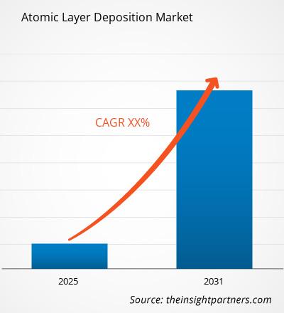
The Atomic Layer Deposition Market was valued at US$ 5.67 Billion in 2025 and is projected to reach US$ 9.69 Billion by 2034, growing at a CAGR of 6.15% during 2026–2034. The market supports atomically controlled thin-film formation for semiconductors, solar devices, medical equipment, and precision electronics where uniformity, conformality, and low-defect interfaces influence device performance.
North America remains a strategically important demand center, with the Atomic Layer Deposition Market size supported by advanced logic fabrication, power electronics, university-led nanotechnology programs, and local semiconductor capacity incentives. The region is estimated to expand at a CAGR range of 5.8–6.2% during 2026–2034, helped by rising use of plasma-enhanced processing and thin films for quantum, compound semiconductor, and medical-device coating applications.
Atomic Layer Deposition Market Assessment and Insights
- North America: The region accounts for 27–31% share in 2025 and grows at a CAGR range of 5.8–6.2% during 2026–2034, led by foundry investments, advanced packaging, and high-value research tools.
- US: The country represents 78–82% of North America in 2025 and grows at a CAGR range of 5.9–6.3% during 2026–2034, driven by leading-edge logic, quantum research, and domestic fab incentives.
- Europe: The region holds 21–25% share in 2025 and grows at a CAGR range of 5.2–5.6% during 2026–2034, with Germany, the Netherlands, France, Finland, and the UK leading demand.
- Asia Pacific: The region holds 36–40% share in 2025 and grows at a CAGR range of 6.8–7.2% during 2026–2034, led by China, Japan, South Korea, Taiwan, India, and Singapore.
- Largest Segment: Semiconductor and Electronics holds 58–62% market share in 2025 and grows at a CAGR range of 6.2–6.6% during 2026–2034 because advanced nodes need conformal films.
- High Growth Segment: Plasma Enhanced ALD holds 21–25% market share in 2025 and grows at a CAGR range of 7.0–7.4% during 2026–2034 as low-temperature processing gains adoption.
- Key companies analyzed in detail: Applied Materials, Inc.; ASM International N.V.; Entegris, Inc.; Kurt J. Lesker Company; Lam Research Corporation; Oxford Instruments plc; Picosun Oy; Qingdao Sifang SRI Intellectual Technology Co., Ltd.; Tokyo Electron Limited; Veeco Instruments Inc.
Source: The Insight Partners' analysis based on proprietary research, government publications, company annual reports, investor presentations, industry databases, and expert interviews.
Atomic-scale deposition has moved from a specialized research technique into a mainstream manufacturing requirement. Device makers are adding complex three-dimensional structures, narrower interconnects, high-k dielectrics, and protective surface layers that require sequential, self-limiting reactions. Production dynamics are shifting toward cluster tools, tighter precursor delivery, lower contamination tolerance, and more automated recipes that improve wafer-to-wafer consistency while reducing process development time.
The demand for front-end tools will rise due to the need for semiconductor localization, passivation of solar cells, coatings for implantable devices, and compound-semiconductor power devices, all of which require material control. Emerging markets are investing in fabrication facilities, pilot plants, and university clean rooms to minimize dependence on foreign technology. The regulatory environment promoting chip security, energy efficiency, and safe medical devices will help qualify the equipment, but there will be hurdles in throughput and precursors.
Atomic Layer Deposition Market Report Scope
| Report Attribute | Details |
|---|---|
| Market size in 2025 | US$ 5.67 Billion |
| Market Size by 2034 | US$ 9.69 Billion |
| Global CAGR (2026 - 2034) | 6.15% |
| Historical Data | 2021-2024 |
| Forecast period | 2026-2034 |
Atomic Layer Deposition Market Analysis
The atomic layer deposition market's growth is mainly attributed to transistor scaling, 3D NAND stacking, advanced DRAM, the trend towards power devices, and thin film barriers. According to WSTS, global semiconductor sales were projected to surpass US$700 billion in 2025, indicating higher capital expenditure on wafer fabrication. ALD is used not only in advanced CMOS but also in memory word lines, diffusion barriers, encapsulation, solar cells, and even biomedicine, owing to its angstrom-level accuracy.
The value chain includes precursor suppliers, vacuum systems, chambers, plasma sources, pumps, metrology, wafer handling, service teams, fabs, and device OEMs. Supply dynamics depend on specialty chemicals, thermal budgets, wafer size, chamber cleanliness, and recipe portability. Customers prefer proven platforms because qualification can extend across months, especially when films interact with high-aspect-ratio structures, sensitive substrates, or regulated medical materials.
The competitive dynamics of the Atomic Layer Deposition Market analysis are driven by process knowledge, installed base, applications support, and co-development, not simply by tool hardware. The players in the semiconductor manufacturing and R&D segments include Applied Materials, Inc., ASM International N.V., Lam Research Corporation, Tokyo Electron Limited, and Oxford Instruments plc. For specialized equipment, materials, and geographic considerations, suppliers include Kurt J. Lesker Company, Picosun Oy, Veeco Instruments Inc., Entegris, Inc., and Qingdao Sifang SRI Intellectual Technology Co., Ltd.
The investor's preferences are for fast single-wafer ALD, batch processing for memory, plasma-assisted ALD for low-temperature deposition, and optimizing the material feed to minimize precursor consumption. Strategic positioning within the industry is accomplished through road mapping the needs of customers for gate-all-around transistors, molybdenum metallization, 3D NAND flash memories, compound semiconductors, and quantum devices. Companies strong in chemistry, field services, and recipe transfer will manage to keep their prices stable during recessions.
● REPORT CUSTOMIZATION
Tailor This Report To Align With Your Specific Business Requirements
This report can be customized to align precisely with your business objectives, scope, and target markets. Customization options include tailored segmentation, geography, competitive analysis, and strategic insights to support informed decision-making.
Customize This Report →WHAT YOU CAN ADJUST
- ● Segmentations
- ● Geography
- ● Competitive Analysis
- ● Language Preferences
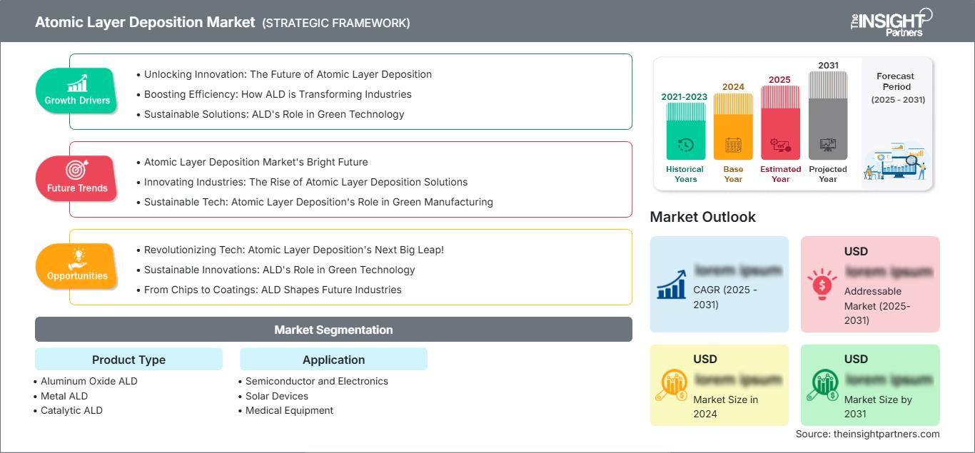
Atomic Layer Deposition Market: Strategic Insights
Regional Insights
North America Atomic Layer Deposition Market
North America holds 27–31% share in 2025 and is projected to grow at a CAGR range of 5.8–6.2% during 2026–2034. The Atomic Layer Deposition Market share in this region includes logic fabs in the U.S., microelectronics for defense purposes, coatings for medical devices, quantum initiatives, and prototyping centers under the CHIPS Act.
Regional purchases will be made based on process reproducibility, contamination avoidance, quick delivery, and compatibility with 200mm and 300mm wafer manufacturing. The Canadians will purchase equipment for applications in photonics, the energy sector, and nanofabrication in academia, whereas Mexicans will purchase equipment used for electronic assembly and power device packaging. Although high equipment prices and a shortage of ALD engineers have been limiting expansion, there is abundant domestic capacity.
U.S. Atomic Layer Deposition Market
The U.S. represents 78–82% of North America in 2025 and is expected to grow at a CAGR range of 5.9–6.3% during 2026–2034. Demand is anchored by foundry logic, advanced packaging, defense electronics, compound semiconductors, and laboratory-to-fab programs. Applied Materials, Inc., Lam Research Corporation, Entegris, Inc., Kurt J. Lesker Company, Oxford Instruments plc, and Veeco Instruments Inc. maintain strong U.S. commercial or application presence.
Application domains include metal gate stacks, molybdenum contacts, silicon nitride films, high-k dielectric films, battery-coating materials, and biocompatible surfaces. Universities and national-level microelectronics facilities are acquiring ALD equipment to bridge the gap between prototyping and pilot production. Fab plants prefer to use ALD equipment that enables complex film processing with foolproof recipes, as any misstep can cause node qualification failure.
Europe Atomic Layer Deposition Market
Europe holds 21–25% share in 2025 and is forecast to grow at a CAGR range of 5.2–5.6% during 2026–2034. Europe is dominated by Germany, owing to automotive power electronics, industrial sensors, research organizations, and compound semiconductor development. The Netherlands provides support via equipment ecosystems and ASM International N.V., while Finland provides expertise in ALD through Picosun Oy.
The UK provides support through the development of quantum, photonics, and plasma-processing applications, with Oxford Instruments plc supplying tools for laboratory and pilot-line applications. France, Italy, and Spain provide demand for microelectronics, aerospace, energy, and medical devices. In Europe, customers focus on efficiency, traceable materials, and reliable products due to stringent qualification processes, which makes ALD an important coating process.
APAC Atomic Layer Deposition Market
Asia Pacific holds 36–40% share in 2025 and is projected to grow at a CAGR range of 6.8–7.2% during 2026–2034. The leading country in the Asia-Pacific is China due to demand for memory, logic, display, and solar devices, and the localization of domestic tools. Japan and South Korea will support growth through memory technology, materials know-how, and equipment provided by Tokyo Electron Limited.
Taiwan will continue to play an important role in the integration of foundry processes, whereas India and Singapore will build assembly, pilot, and specialty wafer fabrication facilities. Australia will be important owing to research, energy, and mining technology. The rapidly developing region will be APAC, driven by government-funded wafer fabrication facilities, high electronics manufacturing, and the expansion of solar fabrication.
Middle East & Africa Atomic Layer Deposition Market
The Middle East & Africa market is forecast to grow at a CAGR range of 5.0–5.4% during 2026–2034. Saudi Arabia is the leading country as smart infrastructure, energy diversification, university research, and electronics localization increase demand for surface engineering. The UAE supports cleanrooms, photonics, and data-center-adjacent research.
The contributions from South Africa include mining sensors, energy systems, and nanotechnology at universities, whereas the rest of MEA’s demand continues to be driven by imported equipment for research and specialty coatings. The growth depends on skilled personnel, service availability, and the availability of precursors. There is potential in energy and infrastructure applications.
Segmentation Analysis
Product Type
Product Type is projected to grow at a CAGR range of 6.0–6.4% during 2026–2034. The Atomic Layer Deposition Market scope by Product Type considers the requirement to optimize process throughput, film chemistry, thermal budget, and substrate sensitivities. Aluminum oxide is one of the most commonly utilized oxides. Metal ALD is used for high-performance interconnects, catalytic ALD increases surface chemistries, and plasma-enhanced ALD enables low-temperature film deposition.
- Aluminum Oxide ALD: The wide use of aluminum oxide is justified by its stable chemistry, strong conformality, and compatibility with electronics, solar, and medical substrates.
- Metal ALD: The strategic importance of Metal ALD lies in the application of this product for contacts, barriers, liners, electrodes, and interconnects, where low resistance, void-free filling, and atomic-level precision are essential.
- Catalytic ALD: Catalytic ALD enables special surface reactions, selective film formation, and low-temperature deposition, which are important for research and development, sensors, catalysts, and temperature-sensitive substrates.
- Plasma Enhanced ALD: Plasma Enhanced ALD makes it possible to increase film density and reactivity and deposition at lower temperatures, which is useful for compound semiconductors, quantum devices, polymers, and advanced packaging applications.
Application
The application is expected to grow at a CAGR of 6.1–6.5% during 2026–2034. Semiconductor and electronics dominate applications as their structures need conformal films within trenches, vias, nanosheets, and stacked memory cells. The solar application uses ALD for passivation and selective coating, whereas the medical equipment industry benefits from ALD coatings that provide protection, biocompatibility, and corrosion resistance.
- Semiconductor and Electronics: Semiconductor & electronics are a leading category, with demand driven by applications such as logic, memory, RF, sensors, and power devices. Thin films for dielectric, barrier, passivation, contact, and encapsulation purposes are required in these devices.
- Solar Devices: ALD is used in the production of solar devices for passivation, durability, and interface improvement, where thinner film coatings increase device efficiency with minimal added cost.
- Medical Equipment: Protective coatings and surfaces of implants and sensors are examples of ALD applications in medical equipment.
Opportunity Snapshot
| Application | Revenue Contribution | Trend Tag | Adoption Stage |
| Semiconductor and Electronics | High | GAA Films | Mature |
| Solar Devices | Medium | Cell Passivation | Scaling |
| Medical Equipment | Medium | Bio Coatings | Emerging |
Atomic Layer Deposition Market Growth Drivers and Impact Analysis
Advanced Semiconductor Scaling Requires Atomic Precision
Current-generation logic and memory components incorporate 3-D structures, thin contacts, advanced gate stacks, and high-aspect-ratio features that can only be effectively coated by conventional deposition. In 2nm or beyond gate-all-around transistors, there may be hundreds of steps in the fabrication process, and therefore, a uniform coating is necessary for consistent electrical behavior. Atomic Layer Deposition allows semiconductor manufacturers to deposit dielectrics, metals, and interfacial layers on complex geometries with precise control over film thickness. These consequences for the business include greater equipment productivity per fab module, greater cooperation from suppliers during the integration process, and increasing demand for integrated solutions for deposition, etching, treatment, and metrology operations. With AI processors and high-bandwidth memory pushing performance demands, atomic-level control is necessary in the production process.
Solar and Energy Devices Need Durable Thin Films
Growing energy applications require conformal coating solutions to enhance the interfacial properties, stability, and longevity of devices. IEA statistics show that solar energy remains one of the fastest-growing sources of electrical power, motivating the development of more efficient cells and module materials. ALD technology can deposit very thin layers of aluminum oxide and other materials for passivation, moisture resistance, and interfacial selectivity, with minimal material waste. The greatest potential of the solution lies in high-end solar cells, transferring innovations from research to production, and in novel battery- or hydrogen-based interfaces that require nanometer-thick films to prevent degradation. Equipment suppliers that offer scalable recipes and lower precursor consumption can address manufacturers seeking efficiency gains without unsustainable cost increases.
Medical and Specialty Devices Require Reliable Surface Engineering
Medical devices, sensing diagnostics, and implanted devices all need to be coated to protect against corrosion, control interfacial bio-reactions, and continue functioning even at miniature dimensions. The reason for using ALD is that it enables the deposition of coatings on complex surfaces, porous substrates, and MEMS structures through controlled chemistry. The effect is not solely based on volume per unit; regulated uses emphasize the need for reliability, recordkeeping, and reproducibility. Manufacturers will enjoy longer periods to qualify a coating, as it will be included in validated designs. The need to miniaturize medical devices, sensors, and laboratory chips further drives demand.
Atomic Layer Deposition Market Future Trends
Selective and Area-Controlled Deposition Moves Toward Production
The Atomic Layer Deposition Market trends technology is expected to include selective ALD processes performed only where the film needs to be deposited, thus eliminating subsequent etching steps and reducing waste. Such methods may prove useful for improving patterning, overlay accuracy, and device miniaturization beyond what pure lithography can achieve. The implementation of such a technique would initially take place in advanced laboratories and pilot plants, followed by large-scale production of logic and memory once its selectivity, defect control, and reliability have been demonstrated. There is ongoing competition among manufacturers of such equipment in surface preparation, inhibitor chemistry, plasma treatment, and in-situ monitoring.
Plasma-Enhanced Processes Expand Beyond Semiconductors
Plasma-enhanced ALD will continue to advance in the fields of compound semiconductors, quantum devices, flexible electronics, and biomedical coatings due to its ability to deposit dense films at lower temperatures. It will be especially important for materials that are sensitive to heat treatment and have better nucleation properties. New-generation devices will involve remote plasma adjustment, cleaner chambers, and recipes for nitride, oxide, and mixed films. Plasma-enhanced ALD technology will become widely spread where precision and efficiency are required.
Atomic Layer Deposition Market Opportunities
Molybdenum and Alternative Metals for Advanced Interconnects
Atomic Layer Deposition Market Forecasts encourage investment in metal deposition alternatives, driven by pushback against tungsten and copper solutions and the scalability issues they face. Molybdenum ALD is gaining significance for contacts, wordlines, and metallization in general due to its ability to reduce resistance and streamline integration in certain designs. Equipment providers can target fabs switching to 3D NAND, advanced DRAM, and gate-all-around logic technologies by offering solutions including low-resistivity films, voidless filling, and process tools compatible with existing systems.
Regional Research Cleanrooms and Pilot Lines
Government-sponsored semiconductor programs are expanding cleanroom capacity beyond existing fabrication centers, creating opportunities for universities, government labs, and pilot fabs to adopt scalable ALD systems. The end users need systems that allow them to work with different materials, enable quick recipe changes, support telepresence, and provide engineering training. The vendors can allocate investments to modular equipment architecture, reduced floor space requirements, services, and process recipes for quantum, photonics, sensors, and compound semiconductors. The attractiveness of the business proposition lies in the fact that early adopters can become influencers of future production requirements.
Recent Developments
- May 2026: Oxford Instruments partners with NYU Nanofab to pioneer atomic-scale quantum advancements with PlasmaPro ASP. The PlasmaPro ASP ALD system is designed for producing superconducting nitrides essential for quantum applications, offering deposition rates three times faster than alternatives.
- April 2026: Applied Materials, Inc. introduced two chipmaking systems designed to create the smallest features in the world’s most advanced logic chips. By controlling materials deposition with atomic-level precision, the technologies enable chipmakers to build faster and more power-efficient transistors at the scale required to sustain the pace of today’s global AI infrastructure buildout.
- February 2026: Forge Nano, Inc., a technology company pioneering domestic battery and semiconductor innovations, announced a breakthrough that fundamentally redefines the economics and architecture of advanced semiconductor manufacturing. The company has demonstrated high-speed, defect-free atomic layer deposition (ALD) coatings in semiconductor features at a 1000:1 aspect ratio. Conformality is maintained at production scale while providing coverage on features 2 orders of magnitude greater than line-of-sight techniques.
Frequently Asked Questions

- Comprehensive Market Sizing and Forecast Analysis
- Detailed Segmentation Analysis
- In-Depth Market Dynamics Assessment
- Regional and Country-Level Insights
- Competitive Landscape and Company Benchmarking
- Strategic Business Intelligence
Recent Reports
Testimonials

The Insight Partners' SCADA System Market report is comprehensive, with valuable insights on current trends and future forecasts. The team was highly professional, responsive, and supportive throughout. We are very satisfied and highly recommend their services.
RAN KEDEM Partner, Reali Technologies LTDs
I requested a report on a very specific software market and the team produced the report in a few days. The information was very relevant and well presented. I then requested some changes and additions to the report. The team was again very responsive and I got the final report in less than a week.
JEAN-HERVE JENN Chairman, Future Analytica
We worked with The Insight Partners for an important market study and forecast. They gave us clear insights into opportunities and risks, which helped shape our plans. Their research was easy to use and based on solid data. It helped us make smart, confident decisions. We highly recommend them.
PIYUSH NAGPAL Sr. Vice President, High Beam Global
The Insight Partners delivered insightful, well-structured market research with strong domain expertise. Their team was professional and responsive throughout. The user-friendly website made accessing industry reports seamless. We highly recommend them for reliable, high-quality research services
YUKIHIKO ADACHI CEO, Deep Blue, LLC.
This is the first time I have purchased a market report from The Insight Partners.While I was unsure at first, I visited their web site and felt more comfortable to take the risk and purchase a market report.I am completely satisfied with the quality of the report and customer service. I had several questions and comments with the initial report, but after a couple of dialogs over email with their analyst I believe I have a report that I can use as input to our strategic planning process.Thank you so much for taking the extra time and making this a positive experience.I will definitely recommend your service to others and you will be my first call when we need further market data.
JOHN SUZUKI President and Chief Executive Officer, Board Director, BK Technologies
I wish to appreciate your support and the professionalism you displayed in the course of attending to my request for information regarding to infectious disease IVD market in Nigeria. I appreciate your patience, your guidance, and the fact that you were willing to offer a discount, which eventually made it possible for us to close a deal. I look forward to engaging The Insight Partners in the future, all thanks to the impression you have created in me as a result of this first encounter.
DR CHIJIOKE ONYIA MANAGING DIRECTOR, PineCrest Healthcare Ltd.Reason to Buy
- Informed Decision-Making
- Understanding Market Dynamics
- Competitive Analysis
- Identifying Emerging Markets
- Customer Insights
- Market Forecasts
- Risk Mitigation
- Boosting Operational Efficiency
- Strategic Planning
- Investment Justification
- Tracking Industry Innovations
- Aligning with Regulatory Trends





 Get Free Sample for