
Chemical Mechanical Planarization Market Size, Share & Demand by 2034
Coverage: By Type (CMP Equipment, CMP Consumable); Application (Integrated Circuits, Mems Nems, Compound Semiconductors, Optics, Others) , and Geography (North America, Europe, Asia Pacific, and South and Central America)
- Status : Data Released
- Report Code : TIPRE00005257
- Category : Electronics and Semiconductor
- No. of Pages : 150
- Available Report Formats :


- Last update date : July 21, 2026


2025 Market Size
US$ 7.20 Bn
Base year value
2034 Forecast
US$ 12.98 Bn
Projected by 2034
CAGR 2026-2034
6.78 %
Growth rate
Addressable Market
US$ 91.25 Bn
(2026-2034)
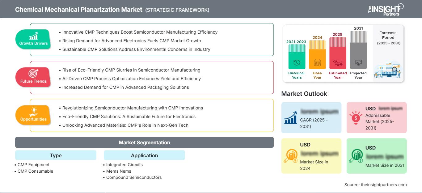
The Chemical Mechanical Planarization market was valued at US$ 7.20 Billion in 2025 and is projected to reach US$ 12.98 Billion by 2034, registering a CAGR of 6.78% during 2026–2034. The market is anchored in semiconductor wafer fabrication, where polishing tools, slurries, pads, cleaning systems, and process-control technologies help fabs achieve uniform surfaces for multilayer integrated circuits, compound semiconductors, MEMS NEMS devices, and precision optics.
North America Chemical Mechanical Planarization Market size is expected to expand at a CAGR of 6.1–6.8% during 2026–2034, supported by semiconductor reshoring, CHIPS Act-linked fab investment, advanced packaging capacity, and demand for locally qualified consumables. The region benefits from strong process engineering talent, equipment supplier presence, and procurement strategies that favor resilient wafer-fabrication supply chains.
Chemical Mechanical Planarization Market Assessment and Insights
- North America held 23–27% share in 2025 and is growing at a CAGR of 6.1–6.8% during 2026–2034, supported by new fabs, advanced packaging, and local consumables qualification.
- US represented 78–82% of North American revenue in 2025 and is growing at a CAGR of 6.2–6.9% during 2026–2034, led by logic and memory investment.
- Europe accounted for 15–19% share in 2025 and is growing at a CAGR of 5.4–6.2% during 2026–2034, with Germany, France, Italy, the UK, and Spain supporting semiconductor and optics demand.
- Asia Pacific held 48–52% share in 2025 and is growing at a CAGR of 7.1–7.9% during 2026–2034, led by China, Taiwan, Japan, South Korea, and India.
- Largest Segment CMP Consumable held 58–62% market share in 2025 and is growing at a CAGR of 6.9–7.6% during 2026–2034 as slurry and pad usage scales with wafer starts.
- High Growth Segment Compound Semiconductors represented 9–12% market share in 2025 and is growing at a CAGR of 8.0–9.2% during 2026–2034, helped by SiC, GaN, and power-device demand.
- Key companies analyzed in detail: Air Products and Chemicals, Inc.; Applied Materials, Inc.; Entegris, Inc.; Ebara Corporation; Fujimi Incorporated; Resonac Holdings Corporation; Lam Research Corporation; Lapmaster Wolters GmbH; Okamoto Machine Tool Works, Ltd.; Revasum, Inc.
Source: The Insight Partners' analysis based on proprietary research, government publications, company annual reports, investor presentations, industry databases, and expert interviews.
Wafer planarization has moved from a back-end polishing step into a strategic yield enabler for advanced semiconductor manufacturing. Within the Chemical Mechanical Planarization Market, growth is reinforced by more interconnect layers, tighter lithography focus windows, rising 300 mm wafer utilization, and greater use of heterogeneous integration. There is an evolution in production dynamics where the synergy among equipment manufacturers, slurry suppliers, pads manufacturers, fabs, and metrology service providers is increasing because of challenging defectivity goals.
Future requirements will be influenced by logic technologies below 3nm, high bandwidth memory technologies, silicon carbide power semiconductor devices, and next-generation packaging technology with surface uniformity demands over dissimilar surfaces. Geographical expansion will bring additional fab capacity, and environment-related regulations will raise issues like slurry disposal, water usage, and consumables recycling.
Chemical Mechanical Planarization Market Report Scope
| Report Attribute | Details |
|---|---|
| Market size in 2025 | US$ 7.20 Billion |
| Market Size by 2034 | US$ 12.98 Billion |
| Global CAGR (2026 - 2034) | 6.78% |
| Historical Data | 2021-2024 |
| Forecast period | 2026-2034 |
Chemical Mechanical Planarization Market Analysis
Chemical Mechanical Planarization growth is driven by rising wafer starts, advanced-node process complexity, and the expansion of memory, logic, and power semiconductor capacity. Demand concentrates where surface non-uniformity can reduce lithography accuracy, increase defect density, or lower device yield. Fabs also require more repeatable polishing performance as copper, tungsten, oxide, low-k dielectric, and emerging materials coexist across complex layer stacks.
The value chain includes equipment makers, slurry and pad suppliers, specialty chemical producers, endpoint detection providers, wafer fabs, OSATs, and engineering service partners. Within the Chemical Mechanical Planarization Market, supply dynamics are influenced by abrasive quality, pad conditioning performance, cleanroom logistics, chemical purity, and qualification cycles. Semiconductor manufacturers increasingly evaluate total cost per wafer because polishing rate, defectivity, downtime, and waste handling determine actual process economics.
CMP market analysis reveals a competitive scenario characterized by platform tools, consumables, wafer handling, and customized polishing equipment. Applied Materials, Inc. and Ebara Corporation are key players in the CMP tool market, whereas Entegris, Inc., Fujimi Incorporated, Resonac Holdings Corporation, and Air Products and Chemicals, Inc. contribute to the supply of materials, slurries, and process purity.
Current investment scenarios emphasize better process control, lower-defect consumable solutions, sustainable slurry formulations, and equipment enhancements that improve consumable life, throughput, and endpoint accuracy. Lam Research Corporation, Lapmaster Wolters GmbH, Okamoto Machine Tool Works, Ltd., and Revasum, Inc. serve specialized segments, including customized polishing, wafer thinning, advanced packaging, and compound semiconductor manufacturing. In addition, increasing demand for artificial intelligence, high-performance computing, memory devices, and advanced logic chips is driving further innovation in CMP technologies. Strategic decision-making will increasingly be influenced by extended fab qualification timelines, material consistency, cost-of-ownership considerations, and proven performance in high-volume manufacturing environments. Suppliers that can deliver superior planarization performance, lower defect rates, reduced chemical consumption, and strong technical support will be better positioned to secure long-term partnerships with leading semiconductor manufacturers and expand their presence across the global Chemical Mechanical Planarization Market.
● REPORT CUSTOMIZATION
Tailor This Report To Align With Your Specific Business Requirements
This report can be customized to align precisely with your business objectives, scope, and target markets. Customization options include tailored segmentation, geography, competitive analysis, and strategic insights to support informed decision-making.
Customize This Report →WHAT YOU CAN ADJUST
- ● Segmentations
- ● Geography
- ● Competitive Analysis
- ● Language Preferences
Chemical Mechanical Planarization Market: Strategic Insights
Regional Insights
North America Chemical Mechanical Planarization Market
North America accounted for 23–27% of the Chemical Mechanical Planarization Market share in 2025 and is projected to expand at a CAGR of 6.1–6.8% during 2026–2034. The demand drivers include logic, memory, compound semiconductors, and advanced packaging, with domestic material sources taking precedence in qualifying the pads, slurries, conditioners, and chemicals.
Fabs in the region rely on CMP to enhance yield uniformity and to help in making multilayer interconnects. The United States is the demand epicenter in the region, with Canada and Mexico contributing to the demand from their involvement in electronics manufacturing, materials distribution, and fab services.
U.S. Chemical Mechanical Planarization Market
The U.S. represented 78–82% of North American revenue in 2025 and is expected to grow at a CAGR of 6.2–6.9% during 2026–2034. Application trends center on integrated circuits, high-bandwidth memory, advanced packaging, silicon carbide power devices, and process modules that require stable removal rates and low defectivity.
Applied Materials, Inc., Air Products and Chemicals, Inc., Entegris, Inc., and Lam Research Corporation support U.S. demand through equipment, materials, services, and fab relationships. Purchasers prioritize process repeatability, chemical purity, uptime, and local technical support because CMP steps directly affect yield learning, wafer cost, and customer qualification schedules.
Europe Chemical Mechanical Planarization Market
Europe held 15–19% share in 2025 and is projected to grow at a CAGR of 5.4–6.2% during 2026–2034. Germany is the leading country, supported by semiconductor equipment ecosystems, automotive electronics, power devices, optics, and industrial automation. France adds demand through microelectronics clusters, while Italy, Spain, and the UK contribute through compound semiconductors and photonics.
European customers emphasize traceable chemicals, lower waste, energy-efficient fabs, and secure supply chains. Public semiconductor initiatives are improving capacity visibility, but qualification timelines remain disciplined because process changes can affect yield. CMP suppliers that combine local service, proven consumables, and material compliance support are positioned to benefit from gradual regional capacity expansion.
APAC Chemical Mechanical Planarization Market
Asia Pacific accounted for 48–52% share in 2025 and is forecast to grow at a CAGR of 7.1–7.9% during 2026–2034. China, Taiwan, Japan, and South Korea lead through high wafer output, memory manufacturing, foundry scale, and equipment ecosystems.
India and Australia add incremental demand through semiconductor policy, compound semiconductor research, and electronics manufacturing. Regional fabs require large volumes of consumables, rapid technical support, and strong contamination control. Chemical Mechanical Planarization remains most intensive in advanced logic, 3D NAND, DRAM, and packaging lines where layer counts and yield targets are high.
Middle East & Africa Chemical Mechanical Planarization Market
The Middle East & Africa market is projected to grow at a CAGR of 4.8–5.6% during 2026–2034. Saudi Arabia and the UAE lead regional interest through technology investment, cleanroom infrastructure, and industrial diversification programs linked to electronics and advanced manufacturing.
South Africa and the rest of MEA contribute through research, optics, and electronics assembly rather than large-scale wafer fabrication. Adoption depends on capital availability, skilled process engineers, and access to qualified suppliers. Early opportunities are likely in specialty substrates, MEMS NEMS prototyping, and regional service partnerships.
Segmentation Analysis
Type
Type is projected to grow at a CAGR of 6.5–7.3% during 2026–2034. The Chemical Mechanical Planarization scope covers capital equipment and recurring consumables that work together to deliver wafer-level flatness. Equipment spending follows new fab and technology-node cycles, while consumables generate repeat demand from slurry, pads, conditioners, and cleaning materials used in every qualified polishing step.
- CMP Equipment supports polishing, cleaning, wafer handling, endpoint control, and process automation. Demand rises with new fab capacity, advanced packaging, and process modules requiring stable removal rates.
- CMP consumables lead to recurring revenue because slurries, pads, and conditioners are consumed continuously during wafer processing. Suppliers compete on defect reduction, selectivity, purity, and qualification reliability.
Application
Application is forecast to grow at a CAGR of 6.8–7.6% during 2026–2034. Integrated circuits remain the largest use case because each advanced device requires repeated planarization across conductor and dielectric layers. MEMS NEMS, compound semiconductors, and optics add specialized demand where substrate quality, surface roughness, and material selectivity determine device performance.
- Integrated Circuits dominate adoption because logic, memory, and packaging structures need uniform surfaces across many layers. Demand follows wafer starts, node transitions, and defectivity requirements.
- Mems Nems require controlled polishing for microstructures, sensors, actuators, and precision devices. Growth is tied to automotive sensing, medical devices, RF components, and miniaturized systems.
- Compound Semiconductors are expanding with SiC and GaN power devices, RF electronics, and photonics. CMP supports substrate preparation, wafer thinning, and defect management.
- Optics uses polishing technologies for lenses, substrates, precision glass, and photonic components. Demand is linked to imaging, AR VR, lasers, and high-performance optical systems.
Opportunity Snapshot
| Application | Revenue Contribution | Trend Tag | Adoption Stage |
| Integrated Circuits | High | Layer Scaling | Mature |
| Mems Nems | Medium | Sensor Precision | Scaling |
| Compound Semiconductors | Medium | SiC Power | Scaling |
| Optics | Low | Photonics Finish | Emerging |
Chemical Mechanical Planarization Market Growth Drivers and Impact Analysis
Advanced-node manufacturing increases polishing intensity
As the size of the features becomes smaller, the need for higher planarity during the manufacture of advanced-node logic and memories increases due to a decrease in focus margins of lithography. An additional layer of interconnection leads to the need for an additional step of polishing and thereby leads to the need for equipment, pads, slurries, and endpoint control. The effect on the market is obvious - fabs will not achieve acceptable yields without a consistent removal rate and low scratching. Companies able to prove their process capability in copper, tungsten, oxide, and low-k layers will have better qualifying chances.
Advanced packaging expands non-front-end demand
The rise in the requirement of planarization due to heterogeneous integration, chiplets, wafer-level packaging, and high bandwidth memory goes beyond the usual front-end wafer fabrication process requirements. Polishing of wafers is required for redistribution layer processes, bonding surfaces, through-silicon vias, and wafer thinning processes. Hence, the customer base for Chemical Mechanical Planarization goes beyond the leading-edge logic fabrication facilities. It becomes particularly significant for the foundries and memory manufacturers who require high capacity and yet maintain bonding performance.
Consumable innovation lowers defects and waste
The slurry and pad advances are increasingly becoming an important factor in purchase decisions because the processing window has to maintain a balance between removal rate, selectivity, surface finish, and defectivity. The fabs are also facing challenges in minimizing the generation of wastewater, minimizing abrasive usage, and minimizing variations in chemicals. Reduced abrasive slurries, increased life spans of pads, advanced conditioners, and improved filtration can lower the cost per wafer processed while ensuring sustainability at the same time. This market effect is cyclical due to the continuous replacement of consumables specific to each layer.
Chemical Mechanical Planarization Market Future Trends
AI-enabled process control moves into CMP modules
Chemical Mechanical Planarization Market trends point toward greater use of AI-enabled endpoint detection, predictive pad conditioning, and model-based recipe adjustment. Future generations will rely on sensor information, metrology feedback, and historical data from wafers to eliminate variations prior to any defect formation. It is important to mention the fact that modern fabs require a more rapid yield learning experience and reduced process excursions. Vendors who incorporate analysis functionality into their tools and consumables programs could provide tangible benefits in terms of higher uptime, pad life, and wafer uniformity.
Sustainable CMP chemistries gain qualification priority
Sustainability will influence future procurement, as fabs measure their consumption of water, slurry handling, chemical toxicity, and cleanroom energy efficiency. In qualification, the emphasis will shift to components that provide effective removal capability, but at the same time minimize the waste processing burden. Reusability of pads, abrasive slurries, and filtration can help in this regard. This process will happen slowly because fabs are reluctant to change any process that could jeopardize their yield rate; however, vendors that have proven life cycle benefits can gain an edge in this environment.
Chemical Mechanical Planarization Market Opportunities
Localized consumable supply for new fabs
Chemical Mechanical Planarization Market Forecasts support investment in regional consumable capacity near new semiconductor fabs. Local mixing, storage, quality control and technical support services will help shorten lead times and ensure supply chain for slurries, pads, conditioners and high-purity chemicals. The best chance to capitalize on this is in North America and Europe, where there are policy-driven fabs looking for robust supply chains. There is an opportunity for suppliers to add value through reliable logistics and application engineering expertise.
Compound semiconductor polishing platforms
The production of compound semiconductors represents a promising field because silicon carbide and gallium nitride-based devices need hard substrate preparation and strict surface quality management. Power electronics, electric cars, renewable power generation equipment, and radio frequency applications raise the demand for unique polishing processes. Manufacturers of the equipment and its consumables will be able to distinguish themselves by developing special recipes based on the hardness, brittleness, and susceptibility to defects of the material. The opportunity suits those companies that can assist in R&D and mass production of the products.
Recent Developments
- June 2026: Qnity Electronics, Inc. (“Qnity”) (NYSE: Q), a premier technology solutions leader across the semiconductor value chain, announced the expansion of its offerings for chemical mechanical planarization (CMP) with the introduction of Optivision Max polishing pads. As semiconductor devices continue to shrink and increase in complexity, diverse CMP processes are critical to achieving the precision required for reliable device performance. Optivision Max CMP pads are designed to help manufacturers maintain tighter control across these increasingly demanding process steps.
- September 2025: FUJIFILM Corporation announced the launch of CMP slurry for advanced packaging, enabling the integration of multiple semiconductor chips into a single package. This product has been adopted by a major semiconductor device manufacturer as an essential abrasive for planarizing bonding surfaces in hybrid bonding, one of the advanced packaging technologies key to enhancing AI semiconductor performance.
- March 2025: Alpha HPA continues to expand its capability to supply high-purity alumina materials to the semiconductor industry, with the most recent customer test results and Letter of Intent to meet the surging demand from AI-driven data centers and next-generation power electronics.
Frequently Asked Questions

- Comprehensive Market Sizing and Forecast Analysis
- Detailed Segmentation Analysis
- In-Depth Market Dynamics Assessment
- Regional and Country-Level Insights
- Competitive Landscape and Company Benchmarking
- Strategic Business Intelligence
Recent Reports
Testimonials

The Insight Partners provided valuable market intelligence that supported our global go-to-market strategy. Their team was professional, responsive, and attentive to our feedback, providing thoughtful analysis and helpful methodological clarifications throughout the project.
Junmo Kim Chief Financial Officer (CFO), Enertech Co., Ltd.
The Insight Partners' SCADA System Market report is comprehensive, with valuable insights on current trends and future forecasts. The team was highly professional, responsive, and supportive throughout. We are very satisfied and highly recommend their services.
RAN KEDEM Partner, Reali Technologies LTDs
I requested a report on a very specific software market and the team produced the report in a few days. The information was very relevant and well presented. I then requested some changes and additions to the report. The team was again very responsive and I got the final report in less than a week.
JEAN-HERVE JENN Chairman, Future Analytica
We worked with The Insight Partners for an important market study and forecast. They gave us clear insights into opportunities and risks, which helped shape our plans. Their research was easy to use and based on solid data. It helped us make smart, confident decisions. We highly recommend them.
PIYUSH NAGPAL Sr. Vice President, High Beam Global
The Insight Partners delivered insightful, well-structured market research with strong domain expertise. Their team was professional and responsive throughout. The user-friendly website made accessing industry reports seamless. We highly recommend them for reliable, high-quality research services
YUKIHIKO ADACHI CEO, Deep Blue, LLC.
This is the first time I have purchased a market report from The Insight Partners.While I was unsure at first, I visited their web site and felt more comfortable to take the risk and purchase a market report.I am completely satisfied with the quality of the report and customer service. I had several questions and comments with the initial report, but after a couple of dialogs over email with their analyst I believe I have a report that I can use as input to our strategic planning process.Thank you so much for taking the extra time and making this a positive experience.I will definitely recommend your service to others and you will be my first call when we need further market data.
JOHN SUZUKI President and Chief Executive Officer, Board Director, BK Technologies
I wish to appreciate your support and the professionalism you displayed in the course of attending to my request for information regarding to infectious disease IVD market in Nigeria. I appreciate your patience, your guidance, and the fact that you were willing to offer a discount, which eventually made it possible for us to close a deal. I look forward to engaging The Insight Partners in the future, all thanks to the impression you have created in me as a result of this first encounter.
DR CHIJIOKE ONYIA MANAGING DIRECTOR, PineCrest Healthcare Ltd.Reason to Buy
- Informed Decision-Making
- Understanding Market Dynamics
- Competitive Analysis
- Identifying Emerging Markets
- Customer Insights
- Market Forecasts
- Risk Mitigation
- Boosting Operational Efficiency
- Strategic Planning
- Investment Justification
- Tracking Industry Innovations
- Aligning with Regulatory Trends





 Get Free Sample for