
Thin Layer Deposition Equipment Market Size, Growth & Trends by 2034
Coverage: by Product (Physical vapor deposition (PVD), Chemical vapor deposition (CVD), Atomic layer deposition (ALD)); Application (Semiconductor, Electronic, Computer, Car, Other) , and Geography (North America, Europe, Asia Pacific, and South and Central America)
- Status : Data Released
- Report Code : TIPRE00008885
- Category : Electronics and Semiconductor
- No. of Pages : 150
- Available Report Formats :


- Last update date : July 21, 2026


2025 Market Size
US$ 58.33 Bn
Base year value
2034 Forecast
US$ 140.64 Bn
Projected by 2034
CAGR 2026-2034
10.27 %
Growth rate
Addressable Market
US$ 883.42 Bn
(2026-2034)
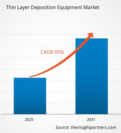
The Thin Layer Deposition Equipment market is expected to rise from US$ 58.33 billion in 2025 to US$ 140.64 billion in 2034 with a CAGR of 10.27% between 2026 and 2034. This growth will be attributed to high-end semiconductors, electronic assemblies, computing hardware, and auto electronics where the control of film is essential for their conductivity, insulation, diffusion barrier, and surface property.
North America continues to remain a vital source of production and research and development and this region’s Thin Layer Deposition Equipment market size is backed by the demand for semiconductor reshoring, defense electronics, artificial intelligence infrastructure, and compound semiconductors. North America is anticipated to see a CAGR of 8.8–9.6% during 2026-2034 as domestic fab plants, universities, and specialized coating companies buy more CVD, PVD, and ALD equipment.
Thin Layer Deposition Equipment Market Assessment and Insights
- North America accounted for 28–31% Thin Layer Deposition Equipment market share in 2025 and is expected to grow at an 8.8–9.6% CAGR between 2026–2034, supported by fab incentives, advanced packaging, and defense-grade electronics capacity.
- US represented 78–82% of North America in 2025 and is projected to expand at an 8.9–9.7% CAGR between 2026–2034, led by foundry, logic, and R&D fabs.
- Europe held 17–20% share in 2025 and may grow at a 7.8–8.6% CAGR between 2026–2034, led by Germany, France, Italy, and the UK in automotive and industrial electronics.
- Asia Pacific captured 43–47% share in 2025 and is forecast to grow at an 11.2–12.1% CAGR between 2026–2034, with China, Japan, South Korea, Taiwan-linked supply chains, and India driving capacity.
- Largest Segment Chemical Vapor Deposition held 39–43% market share in 2025 and is estimated to grow at a 9.6–10.4% CAGR between 2026–2034 due to broad wafer process coverage.
- High Growth Segment Atomic layer deposition held 20–24% market share in 2025 and is projected to grow at a 12.4–13.6% CAGR between 2026–2034 as device geometries tighten.
- Key companies analyzed in detail: AIXTRON SE, Angstrom Engineering Inc., Blue Wave Semiconductors, Inc., Canon Anelva Corporation, CVD Equipment Corporation, Intevac, Inc., Kenosistec S.r.l., Lam Research Corporation, PVD Products, Inc., SAMCO Inc.
Source: The Insight Partners' analysis based on proprietary research, government publications, company annual reports, investor presentations, industry databases, and expert interviews.
The architecture of the tool has evolved from standalone coating chambers to an integrated solution involving plasma control, precursor delivery, metrology feedback loop, and automated wafer transport. This transition is driven by stringent uniformity specifications of films required for logic, memory, power semiconductors, displays, and sensors. The dynamics of production are undergoing transformation as producers try to harmonize high-throughput PVD machines with ALD tools offering conformal films in complex 3D structures and thereby make Thin Layer Deposition Equipment integral to yield management.
Through the forecast period, capital expenditure would spread out into other markets due to localization of chip fabrication and the qualification of electronics by automobile manufacturers for higher reliability. The drive by regulations towards higher efficiency, material traceability, and emission reduction is likely to favor equipment with better gas utilization, more efficient cleaning systems of chamber and digital process control. The emergence of new fabs in India, the United States, and some European countries may diversify customers.
Thin Layer Deposition Equipment Market Report Scope
| Report Attribute | Details |
|---|---|
| Market size in 2025 | US$ 58.33 Billion |
| Market Size by 2034 | US$ 140.64 Billion |
| Global CAGR (2026 - 2034) | 10.27% |
| Historical Data | 2021-2024 |
| Forecast period | 2026-2034 |
Thin Layer Deposition Equipment Market Analysis
The Thin Layer Deposition Equipment market growth is supported by an increase in wafer fab equipment spending, AI accelerator manufacture, high bandwidth memory requirements, and power semiconductors. SEMI forecasted semiconductor manufacturing equipment sales of US$ 125.5 billion for 2025 and wafer fab equipment sales of US$ 110.8 billion, suggesting a robust capital expenditure base for deposition systems.
The supply chain involves vacuum components, plasma generation devices, precursors, targets, chambers, software, process recipes, and maintenance services. The supply side is still influenced by specialty gases, high purity metals, ceramics, valves, and controls, while the customer side values uptime, process reproducibility, and tool compatibility between multiple fabs.
Thin Layer Deposition Equipment Market analysis indicates a competitive environment driven by economies of scale, installed base, application expertise, and service capabilities. Lam Research Corporation competes with high-volume semiconductor process equipment, whereas AIXTRON SE competes with compound semiconductor and specialty epitaxy equipment. Canon Anelva Corporation, SAMCO Inc., and Intevac, Inc. cater to vacuum deposition market segments associated with electronics, displays, and thin film applications.
Specialty vendors like Angstrom Engineering Inc., Blue Wave Semiconductors, Inc., CVD Equipment Corporation, Kenosistec S.r.l., and PVD Products, Inc. contribute to the market with their customizable research, pilot, and production systems. Strategic positioning increasingly relies on process development partnership, chamber design customization, lifecycle support, and capability of handling new materials.
● REPORT CUSTOMIZATION
Tailor This Report To Align With Your Specific Business Requirements
This report can be customized to align precisely with your business objectives, scope, and target markets. Customization options include tailored segmentation, geography, competitive analysis, and strategic insights to support informed decision-making.
Customize This Report →WHAT YOU CAN ADJUST
- ● Segmentations
- ● Geography
- ● Competitive Analysis
- ● Language Preferences
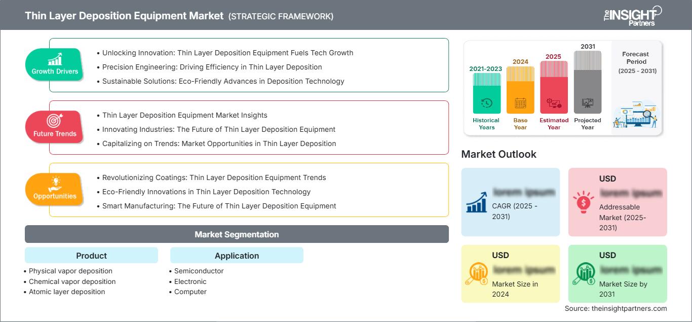
Thin Layer Deposition Equipment Market: Strategic Insights
Regional Insights
North America Thin Layer Deposition Equipment Market
The North American Thin Layer Deposition Equipment market had 28-31% share in 2025 and will see a CAGR of 8.8-9.6% during 2026-2034. This growth driver includes semiconductor reshoring initiatives, defense electronics purchase, and growing chip requirements for data centers in AI. Thin Layer Deposition Equipment's regional strength stems from the US factories that need state-of-the-art films like dielectrics, metals, barriers, and passivations in logic, memory, and compound chips
The buying decisions of regional clients are moving away from acquisition cost towards process stability, chamber performance, and services proximity. The United States is driving demand, while Canada participates via photonics, quantum, and research thin layer deposition equipment applications. Public and private investment in fabs and in equipment replacements for mature-node automotive chips and advanced packaging will help drive sales.
U.S. Thin Layer Deposition Equipment Market
The US accounted for 78–82% of North America Thin Layer Deposition Equipment market in 2025 and is estimated to grow at an 8.9–9.7% CAGR during 2026–2034. Demand is concentrated in foundry, logic, memory, defense, and university nanofabrication facilities. Thin Layer Deposition Equipment is also used in power electronics, RF components, and advanced sensors that support electrified vehicles and industrial automation.
Company presence is strongest through domestic manufacturing, field engineering, and application labs. Lam Research Corporation and Intevac, Inc. provide semiconductor and vacuum-process expertise, while PVD Products, Inc., Blue Wave Semiconductors, Inc., and CVD Equipment Corporation address research-to-production niches. Application trends favor ALD for 3D structures and CVD for scalable dielectric films.
Europe Thin Layer Deposition Equipment Market
Europe accounted for 17% to 20% of Thin Layer Deposition Equipment market in 2025, and is expected to increase at a 7.8% to 8.6% CAGR until 2034. Germany will have the highest adoption rate regionally, because of automotive electronics, power semiconductor applications, industrial sensor usage, and compound semiconductors.
The United Kingdom will contribute through photonics, quantum devices, and scientific instrumentation for prototyping to pilot use, which requires accurate thin-film deposition technologies. France, Italy, and Spain will make contributions through aerospace electronics, microelectronic research, solar production equipment, and specialty coating needs. Energy efficiency, low contamination operation, and supply chain security will drive European purchases.
APAC Thin Layer Deposition Equipment Market
The APAC region accounted for 43-47% share in 2025 and will record an 11.2-12.1% CAGR over 2034 to become the leading region in terms of market size. China dominates in terms of volume consumption, whereas Japan and South Korea continue purchases for memory, display, and advanced material applications.
Australia also accounts due to efforts in research and development, photonics, and materials science. Favorable industrial policies, supply chain localization, and higher tool utilization drive repeat business. The regional buyers are keen on capacity, recipe transfer, chamber availability, and compatibility with high volume fabrication facilities for logic, memory, sensors, and automotive electronics.
Middle East & Africa Thin Layer Deposition Equipment Market
The MEA is anticipated to see a 6.9%-7.8% CAGR over the period 2026-2034, driven by the UAE for its investments and R&D capabilities in the field of electronics. While Saudi Arabia focuses on diversifying industries, South Africa's contribution is evident in academic labs, mining-oriented sensors, and coatings.
MEA's demand is selective but growing, particularly for energy, telecommunications, and infrastructure development, where there is a need for electronics along with coated materials. Equipment adoption is influenced by technical education, availability of services, and collaboration with international universities and OEMs.
Segmentation Analysis
Product
Product is projected to grow at a 9.8–10.8% CAGR during 2026–2034 as fabs select deposition platforms based on film type, thermal budget, conformity, and throughput. The Thin Layer Deposition Equipment scope spans high-volume wafer manufacturing, pilot production, research laboratories, and specialty coating lines serving electronics, computing, automotive, and industrial applications.
- Physical vapor deposition remains important for metal films, hard coatings, seed layers, and optical stacks where line-of-sight deposition, target material flexibility, and high throughput support established production environments.
- Chemical Vapor Deposition is the largest product segment, supported by dielectric films, conductive layers, passivation, and scalable wafer processing across memory, logic, sensors, and electronic component manufacturing.
- Atomic layer deposition is the high-growth product segment because it enables conformal, atomic-scale films on 3D device structures, advanced packaging features, and emerging nanoscale materials.
Application
Application is estimated to grow at a 10.0–11.0% CAGR during 2026–2034, with demand tied to semiconductor scaling, electronic miniaturization, computing performance, and electrified mobility. Buyers prioritize film uniformity, contamination control, repeatability, and process recipes that reduce yield loss across increasingly complex substrates.
- Semiconductor dominates application demand because advanced chips require repeated deposition steps for gate stacks, interconnects, barriers, dielectrics, memory layers, and passivation structures.
- Electronic applications rely on deposition tools for displays, sensors, power components, printed electronics, and miniaturized assemblies where durable thin films improve electrical and optical performance.
- Computer applications are supported by processors, storage, AI accelerators, and high-performance computing hardware that need precise films for speed, reliability, and thermal management.
- Car applications are expanding with electric vehicles, ADAS, power modules, battery electronics, and in-vehicle sensors that require rugged coatings and semiconductor-grade reliability.
Opportunity Snapshot
| Application | Revenue Contribution | Trend Tag | Adoption Stage |
| Semiconductor | High | Advanced Nodes | Mature |
| Electronic | Medium | Smart Devices | Scaling |
| Computer | High | AI Compute | Scaling |
| Car | Medium | EV Power | Scaling |
Thin Layer Deposition Equipment Market Growth Drivers and Impact Analysis
AI and Advanced Logic Capacity Expansion
AI accelerators and high-performance processors require more deposition-intensive process flows than conventional chips because transistor scaling, interconnect density, and packaging complexity all increase film requirements. SEMI reported 2025 wafer fab equipment expectations above US$ 110 billion, demonstrating the capital intensity behind this cycle. Thin Layer Deposition Equipment benefits directly because each advanced node depends on repeatable dielectric, metal, barrier, and passivation layers. The impact is visible in tool qualification schedules, longer service contracts, and demand for process chambers that reduce variability across multiple fabs.
Electrification and Power Device Manufacturing
Electric vehicles, charging infrastructure, renewable integration, and industrial automation are expanding the need for silicon carbide, gallium nitride, insulated-gate bipolar transistor, and sensor devices. These components require controlled films for insulation, contacts, passivation, and thermal performance. Equipment suppliers are responding with reactors and PVD systems suited for compound substrates, thicker films, and lower defect densities. The market impact is a broader customer base beyond leading-edge logic, with automotive-qualified fabs demanding reliability data, uptime guarantees, and long-term process support.
Localization of Semiconductor Supply Chains
National semiconductor programs are creating new demand for process equipment as fabs are planned, built, and qualified in the US, Europe, India, Japan, and parts of Southeast Asia. Localization does not eliminate global sourcing, but it increases the need for regional service teams, training centers, and application engineering. Thin Layer Deposition Equipment vendors that can support recipe transfer and rapid tool matching will gain advantage. This driver also supports smaller research and pilot systems used before commercial fab ramp-up.
Thin Layer Deposition Equipment Market Future Trends
Spatial ALD and Area-Selective Processes
Thin Layer Deposition Equipment market trends will increasingly center on spatial ALD, area-selective deposition, and lower-temperature chemistries that enable precise films without excessive cycle time. These methods are expected to support nanosheet transistors, advanced memory, heterogeneous integration, and sensitive substrates. Future buyers will compare tools on selectivity, precursor efficiency, and defect control rather than chamber count alone. The trend may also reshape supplier partnerships because chemical companies, toolmakers, and fabs must co-optimize materials and process windows earlier in development.
Digital Process Control and Predictive Maintenance
Deposition tools are moving toward integrated sensors, chamber digital twins, and predictive maintenance models that detect drift before yield loss occurs. Future systems will use equipment data to optimize plasma stability, gas flow, temperature uniformity, and target consumption. This shift matters because high-volume fabs cannot tolerate unplanned downtime during AI, memory, and automotive chip ramp-ups. Suppliers with robust analytics and secure connectivity will be better positioned to convert installed bases into recurring service and software revenue.
Thin Layer Deposition Equipment Market Opportunities
Advanced Packaging and Heterogeneous Integration
Advanced packaging creates investment opportunities because chiplets, interposers, redistribution layers, and hybrid bonding require reliable barrier, seed, dielectric, and passivation films. Thin Layer Deposition Equipment Market Forecasts indicate that packaging-related process steps will become more deposition-intensive as AI and high-bandwidth memory architectures scale. Suppliers can target this opportunity with tools optimized for panel-level substrates, low-temperature processes, and uniform coatings over topography. Partnerships with outsourced assembly and test providers may accelerate adoption outside traditional front-end fabs.
Compound Semiconductor and Photonics Capacity
Compound semiconductors and photonics offer an attractive opportunity because 5G, data centers, lidar, power electronics, and optical communication need specialized epitaxy and thin-film stacks. AIXTRON SE, SAMCO Inc., and specialty PVD and CVD suppliers are well positioned where customers require material-specific expertise rather than generic platforms. Investors should monitor capacity additions in silicon carbide, gallium nitride, indium phosphide, and optical coatings. These applications can support premium pricing when film quality, defect control, and application support are differentiated.
Recent Developments
- May 2026: Blue Wave Semiconductors presents a fully customizable, state-of-the-art Pulsed Laser Deposition (PLD) System, engineered for the synthesis of high-quality thin films of metal oxides, nitrides, and complex multilayer device structures. This system is designed to support both fundamental research and advanced materials development, offering precise control over film composition, thickness, and crystalline quality.
- March 2024: Lam Research hopes to revolutionize microchip manufacturing with the launch of a new system: Prestis. Lam is using lasers to deposit thin films and bringing pulsed laser deposition (PLD) to wafer-level mass production. Prestisis expected to be key in developing cutting-edge specialty technologies devices, such as RF (radio frequency) filters for 5G and Wi-Fi 6 and high-end MEMS (micro-electromechanical systems) microphones.
Frequently Asked Questions

- Comprehensive Market Sizing and Forecast Analysis
- Detailed Segmentation Analysis
- In-Depth Market Dynamics Assessment
- Regional and Country-Level Insights
- Competitive Landscape and Company Benchmarking
- Strategic Business Intelligence
Recent Reports
Testimonials

The Insight Partners' SCADA System Market report is comprehensive, with valuable insights on current trends and future forecasts. The team was highly professional, responsive, and supportive throughout. We are very satisfied and highly recommend their services.
RAN KEDEM Partner, Reali Technologies LTDs
I requested a report on a very specific software market and the team produced the report in a few days. The information was very relevant and well presented. I then requested some changes and additions to the report. The team was again very responsive and I got the final report in less than a week.
JEAN-HERVE JENN Chairman, Future Analytica
We worked with The Insight Partners for an important market study and forecast. They gave us clear insights into opportunities and risks, which helped shape our plans. Their research was easy to use and based on solid data. It helped us make smart, confident decisions. We highly recommend them.
PIYUSH NAGPAL Sr. Vice President, High Beam Global
The Insight Partners delivered insightful, well-structured market research with strong domain expertise. Their team was professional and responsive throughout. The user-friendly website made accessing industry reports seamless. We highly recommend them for reliable, high-quality research services
YUKIHIKO ADACHI CEO, Deep Blue, LLC.
This is the first time I have purchased a market report from The Insight Partners.While I was unsure at first, I visited their web site and felt more comfortable to take the risk and purchase a market report.I am completely satisfied with the quality of the report and customer service. I had several questions and comments with the initial report, but after a couple of dialogs over email with their analyst I believe I have a report that I can use as input to our strategic planning process.Thank you so much for taking the extra time and making this a positive experience.I will definitely recommend your service to others and you will be my first call when we need further market data.
JOHN SUZUKI President and Chief Executive Officer, Board Director, BK Technologies
I wish to appreciate your support and the professionalism you displayed in the course of attending to my request for information regarding to infectious disease IVD market in Nigeria. I appreciate your patience, your guidance, and the fact that you were willing to offer a discount, which eventually made it possible for us to close a deal. I look forward to engaging The Insight Partners in the future, all thanks to the impression you have created in me as a result of this first encounter.
DR CHIJIOKE ONYIA MANAGING DIRECTOR, PineCrest Healthcare Ltd.Reason to Buy
- Informed Decision-Making
- Understanding Market Dynamics
- Competitive Analysis
- Identifying Emerging Markets
- Customer Insights
- Market Forecasts
- Risk Mitigation
- Boosting Operational Efficiency
- Strategic Planning
- Investment Justification
- Tracking Industry Innovations
- Aligning with Regulatory Trends





 Get Free Sample for