
3D IC and 2.5D IC Packaging Market Size, Trends & Demand by 2034
3D IC and 2.5D IC Packaging Market Size and Forecasts (2021–2034), Global and Regional Share, Trends, and Growth Opportunity Analysis Report Coverage : By The report is segmented into Packaging Technology (3D Wafer-Level Chip Scale Packaging, 3D TSV and 2.5D), Application (Logic, Memory, MEMS/Sensors, Imaging & Optoelectronics, LED), End-use (Telecommunication, Consumer Electronics, Automotive, Military & Defense, Medical Devices, Others)
- Status : Data Released
- Report Code : TIPRE00039688
- Category : Electronics and Semiconductor
- No. of Pages : 150
- Available Report Formats :


- Last update date : July 15, 2026


2025 Market Size
US$ 135.24 Bn
Base year value
2034 Forecast
US$ 415.51 Bn
Projected by 2034
CAGR 2026-2034
13.28 %
Growth rate
Addressable Market
US$ 2,389.94 Bn
(2026-2034)
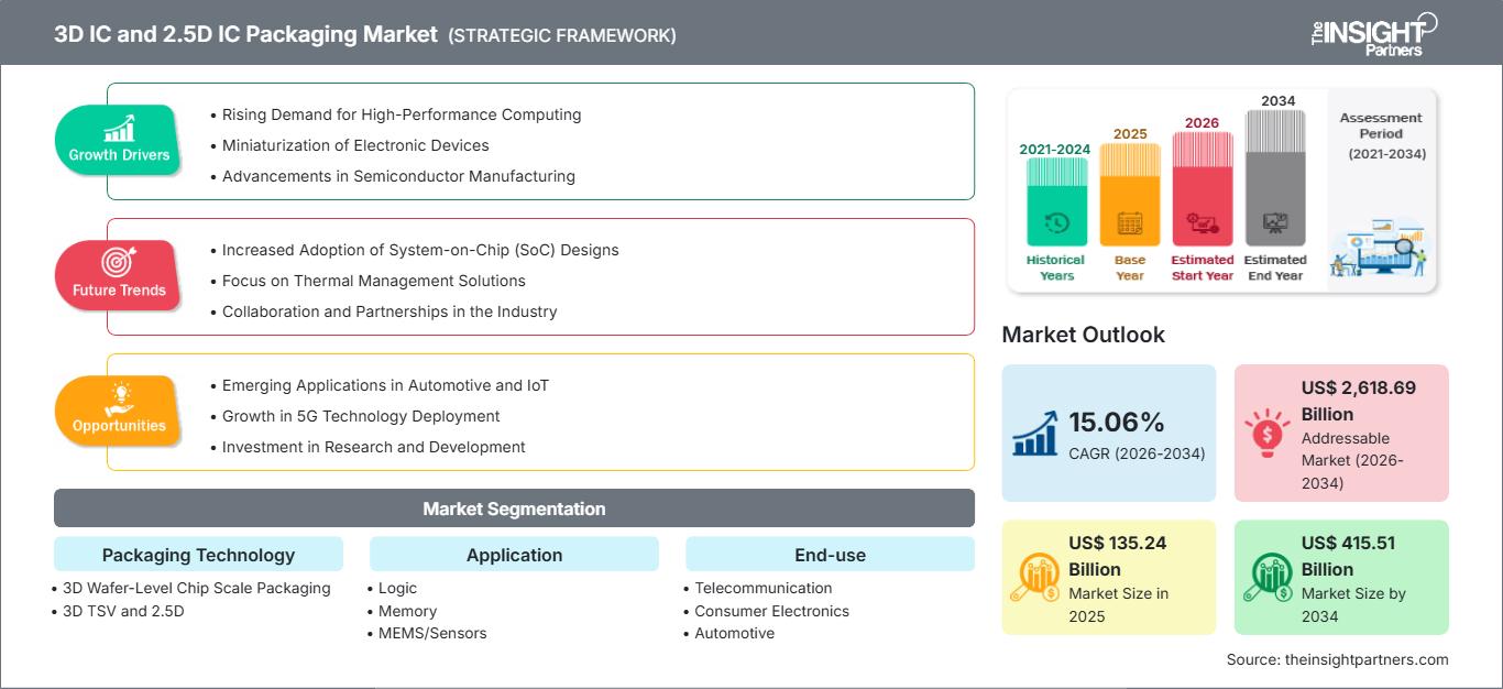
The 3D IC and 2.5D IC Packaging market was valued at US$ 135.24 billion in 2025 and is expected to reach US$ 415.51 billion by 2034; it is estimated to record a CAGR of 13.28% during 2026-2034.
3D IC and 2.5D IC Packaging Market Assessment and Insights
- North America: The region demonstrates strong growth potential with an estimated 26–30% market share in 2025 and is projected to grow at a CAGR of 10–12% during 2026–2034. Demand is driven by advanced semiconductor manufacturing, high-performance computing (HPC), AI accelerators, and defense electronics across the US and Canada.
- US: The US accounts for approximately 80–84% of the North American market in 2025 and is expected to expand at a CAGR of 10–12% from 2026–2034. Strong investments in semiconductor innovation, chiplet architecture, AI processors, and advanced packaging technologies support market growth.
- Europe: Europe represents an estimated 20–24% market share in 2025 and is anticipated to grow at a CAGR of 9–11% during 2026–2034. Germany, France, the UK, Italy, and the Netherlands contribute through automotive semiconductors, industrial electronics, and collaborative semiconductor R&D initiatives.
- Asia Pacific: Asia Pacific holds the largest regional share of approximately 44–48% in 2025 and is expected to register a CAGR of 11–13% during 2026–2034. China, Taiwan, South Korea, Japan, and India lead regional expansion through semiconductor fabrication, outsourced semiconductor assembly and testing (OSAT), consumer electronics manufacturing, and AI chip production.
- Largest Segment: 3D IC Packaging represents the largest segment with a market share of approximately 60–65% in 2025 and is projected to grow at a CAGR of 11–13% during 2026–2034, driven by increasing adoption in high-bandwidth memory (HBM), AI processors, and high-performance computing applications.
- High Growth Segment: 2.5D IC Packaging represents the fastest-growing segment with an estimated market share of 35–40% in 2025 and a CAGR of 12–14% during 2026–2034, supported by growing demand for chiplet-based architectures, advanced interposer technologies, and next-generation data center processors.
- Key companies analyzed in detail: Taiwan Semiconductor Manufacturing Company (TSMC), Samsung Electronics Co., Ltd., Intel Corporation, Amkor Technology, Inc., ASE Technology Holding Co., Ltd., JCET Group Co., Ltd., SPIL (Siliconware Precision Industries Co., Ltd.), Broadcom Inc., Micron Technology, Inc., and SK hynix Inc.
Source: The Insight Partners' analysis based on proprietary research, government publications, company annual reports, investor presentations, industry databases, and expert interviews.
The 3d IC and 2.5d IC Packaging Market forecast reflects a shift from packaging efficiency solutions to a core semiconductor architecture strategy. Since monolithic scaling is getting expensive in terms of investment in technology, packaging is becoming a means to integrate logic, memory, MEMS, sensors, imaging, optoelectronics, and LEDs within the same package. It is clear in applications of artificial intelligence accelerators, smartphones, automotive electronics, telecommunications modules, and defense computing platforms.
Factors influencing the market include increasing demand for 3D TSVs, 2.5D interposers, wafer-level chip scale packaging, and heterogeneous integration. Leading companies such as Samsung Electronics Ltd., Taiwan Semiconductor Manufacturing Company, Ltd., Intel Corporation, ASE Technology Holding Co., Ltd., Amkor Technology, Broadcom, Texas Instruments Inc., United Microelectronics Corporation, JCET Group Co., Ltd., and Powertech Technology Inc. are well-placed in each segment of production, packaging services, design enablement, and end-use markets.
3D IC and 2.5D IC Packaging Market Report Scope
| Report Attribute | Details |
|---|---|
| Market size in 2025 | US$ 135.24 Billion |
| Market Size by 2034 | US$ 415.51 Billion |
| Global CAGR (2026 - 2034) | 13.28% |
| Historical Data | 2021-2024 |
| Forecast period | 2026-2034 |
3D IC and 2.5D IC Packaging Market Analysis
The 3d IC and 2.5d IC Packaging Market is driven by the requirement to place greater computing density, bandwidth, and sensing capability into smaller and more energy-efficient semiconductor packages. Logic and memory integration is particularly important as AI, data center, and mobile processors become more memory-bound. MEMS, imaging, optoelectronics, and LED applications also benefit from compact integration, improved signal integrity, and shorter electrical pathways, contributing to the growth of the 3d IC and 2.5d IC Packaging Market size.
The ecosystem spans wafer fabrication, package design, substrates, interposers, bonding equipment, inspection systems, OSAT providers, materials suppliers, and fabless semiconductor customers. Foundries and IDMs are increasingly aligning packaging roadmaps with chip architecture decisions. ASE Technology Holding Co., Ltd., Amkor Technology, JCET Group Co., Ltd., and Powertech Technology Inc. provide assembly and test scale, while Taiwan Semiconductor Manufacturing Company, Ltd. and Intel Corporation connect packaging to advanced manufacturing roadmaps.
Competition is moving beyond conventional assembly cost toward interconnect density, thermal performance, yield learning, and customer qualification speed. Samsung Electronics Ltd. leverages memory and advanced packaging strengths, while Taiwan Semiconductor Manufacturing Company, Ltd. and Intel Corporation use integrated process-packaging strategies. OSAT leaders compete through flexible capacity, system-in-package expertise, advanced testing, and geographic diversification for customers seeking resilient supply chains.
Investment trends are concentrated around AI packaging bottlenecks, high-density substrates, TSV reliability, hybrid bonding, thermal interface materials, and package-level testing. Strategic positioning depends on whether suppliers can scale complex multi-die packages without compromising reliability. Partnerships between foundries, OSATs, equipment vendors, and fabless chip designers are becoming more important because package design now influences product performance, launch timing, and supply assurance.
● REPORT CUSTOMIZATION
Tailor This Report To Align With Your Specific Business Requirements
This report can be customized to align precisely with your business objectives, scope, and target markets. Customization options include tailored segmentation, geography, competitive analysis, and strategic insights to support informed decision-making.
Customize This Report →WHAT YOU CAN ADJUST
- ● Segmentations
- ● Geography
- ● Competitive Analysis
- ● Language Preferences
3D IC and 2.5D IC Packaging Market: Strategic Insights
Regional Insights
North America 3d IC and 2.5d IC Packaging
North America is projected to expand at an estimated 14%–16% CAGR, supported by semiconductor localization, advanced computing demand, and stronger interest in secure packaging capacity. AI servers, defense electronics, automotive compute modules, and telecom infrastructure are creating demand for package-level performance improvements and geographically resilient back-end manufacturing routes.
Growth is reinforced by Intel Corporation’s advanced packaging roadmap, Amkor Technology’s U.S. capacity plans, and strong fabless demand for high-performance chips. The region benefits from design intensity, policy support, and closer coordination between wafer fabrication, packaging, and end-market qualification, especially for applications where reliability, low latency, and supply security influence procurement decisions.
U.S. 3d IC and 2.5d IC Packaging Market
The U.S. represents an estimated 78%–85% share of North America’s demand and is likely to grow at about 14.5%–16% CAGR. Demand is concentrated in AI accelerators, defense electronics, telecom systems, automotive compute, and medical devices that require compact packages with strong thermal stability and high data throughput, contributing significantly to the 3d IC and 2.5d IC Packaging Market share.
Company presence is led by Intel Corporation, Amkor Technology, Broadcom, Texas Instruments Inc., and Taiwan Semiconductor Manufacturing Company, Ltd.’s U.S.-linked manufacturing ecosystem. Application trends show rising use of 3D packaging in logic, memory, MEMS, sensors, imaging, and optoelectronics as customers seek better performance per watt across cloud, defense, mobility, and healthcare platforms.
Europe 3d IC and 2.5d IC Packaging Market
Europe holds an estimated 13%–17% share of the global market and is projected to grow at about 12.5%–14.5% CAGR. Germany is the leading country because automotive semiconductors, industrial automation, power electronics, and precision manufacturing create sustained demand for reliable multi-die and high-density packaging formats, reflecting key 3d IC and 2.5d IC Packaging Market trends.
The UK market is shaped by semiconductor design, telecom innovation, defense electronics, and compound technology research. Adoption is selective but strategically relevant where advanced packaging supports secure communications, sensors, and specialist computing. Germany remains ahead due to its automotive electronics base, industrial controls, and demand for qualified packaging platforms with long lifecycle reliability.
France, Italy, and Spain contribute through aerospace electronics, medical devices, automotive systems, industrial machinery, and embedded electronics manufacturing. France benefits from defense and semiconductor activity, Italy from industrial automation and automotive components, and Spain from electronics modernization. Regional progress depends on packaging investment, substrate access, equipment partnerships, and stronger links between design centers and outsourced assembly capacity.
APAC 3d IC and 2.5d IC Packaging Market
Asia Pacific leads the 3d IC and 2.5d IC Packaging Market with an estimated 53%–59% global share and a projected 15.5%–17% CAGR. China, Japan, South Korea, India, and Australia contribute through electronics manufacturing, memory, materials, design services, and policy-backed semiconductor programs. Taiwan remains the leading hub due to foundry and OSAT density.
China’s demand is supported by consumer electronics, telecom infrastructure, automotive electronics, and domestic semiconductor localization. Japan and South Korea strengthen the region through memory leadership, precision equipment, advanced materials, and display-related electronics. Their role is critical because 3D packages require reliable substrates, bonding tools, inspection systems, and disciplined high-volume process control.
India is gaining relevance through electronics manufacturing incentives, semiconductor policy support, and emerging advanced packaging investments, while Australia contributes through research, defense electronics, and specialty systems. APAC’s advantage comes from supplier clustering, manufacturing scale, and proximity to smartphone, telecom, automotive, and data center hardware value chains that increasingly depend on heterogeneous integration.
Middle East & Africa 3d IC and 2.5d IC Packaging Market
The Middle East & Africa 3d IC and 2.5d IC Packaging Market is projected to grow at an estimated 11.5%–13.5% CAGR, with the UAE leading regional adoption. Growth is application-led rather than manufacturing-led, supported by data centers, smart cities, telecom modernization, defense systems, and energy-sector digitalization that require advanced semiconductors embedded in imported equipment.
Saudi Arabia and the UAE are expanding AI infrastructure, industrial automation, and connected energy assets, indirectly increasing demand for chips using compact and reliable packages. Energy operations require rugged electronics, power management, communications modules, and sensing systems where advanced packaging can improve durability, power efficiency, and integration density in harsh operating environments.
South Africa and the rest of MEA show demand across mining automation, healthcare equipment, telecommunications, and government digital infrastructure. Regional opportunity will depend on data center growth, system integration capabilities, and strategic imports of advanced electronics. The market’s packaging value is mostly embedded within high-performance devices rather than local high-volume assembly operations.
Segmentation Analysis
Packaging Technology
- 3D Wafer-Level Chip Scale Packaging: 3D Wafer-Level Chip Scale Packaging supports compact consumer, sensor, and mobile devices by reducing package footprint while improving electrical performance, production scalability, and integration density.
- 3D TSV and 2.5D: 3D TSV and 2.5D packaging enable high-bandwidth logic-memory integration, chiplet assembly, and interposer-based designs for AI accelerators, high-performance computing, telecom equipment, and advanced imaging systems.
Application
- Logic: Logic applications use 3D packaging to improve processor density, reduce latency, and support chiplet-based integration for AI, networking, automotive compute, and high-performance edge devices.
- Memory: Memory applications benefit from vertical stacking and TSV-enabled architectures that increase bandwidth, reduce footprint, and support data-intensive workloads across AI, servers, smartphones, and graphics platforms.
- MEMS/Sensors: MEMS/Sensors adoption is driven by compact sensing modules, wearables, automotive safety systems, medical monitoring devices, and industrial automation platforms requiring reliable multi-function integration.
- Imaging & Optoelectronics: Imaging & Optoelectronics use 3D packaging for camera modules, optical communication components, LiDAR, photonics, and advanced sensing systems needing precise alignment and compact electrical pathways.
- LED: LED applications adopt 3D packaging where thermal performance, miniaturization, and integration with control electronics matter for displays, automotive lighting, medical devices, and high-brightness illumination systems.
End-use
- Telecommunication: Telecommunication end-use relies on compact RF, optical, baseband, and network processor packages that improve bandwidth, power efficiency, and signal integrity across 5G and edge infrastructure.
- Consumer Electronics: Consumer Electronics leads adoption through smartphones, wearables, laptops, cameras, and gaming devices requiring thinner designs, higher memory bandwidth, better thermal behavior, and multifunction integration.
- Automotive: Automotive demand is rising as advanced driver assistance, infotainment, electrification, connectivity, and in-vehicle computing require reliable semiconductor packages with robust thermal and lifecycle performance.
- Military & Defense: Military & Defense applications prioritize secure, compact, and rugged packaging for radar, communications, electronic warfare, aerospace electronics, and mission-critical computing systems.
- Medical Devices: Medical Devices use 3D packaging in imaging systems, diagnostics, wearables, implants, and monitoring platforms where miniaturization, low power, reliability, and signal precision are essential.
Opportunity Snapshot
| End-use | Revenue Contribution | Trend Tag | Adoption Stage |
| Telecommunication | High | 5G Edge | Scaling |
| Consumer Electronics | High | Device Miniaturization | Mature |
| Automotive | Medium | ADAS Compute | Scaling |
| Military & Defense | Medium | Secure Systems | Scaling |
| Medical Devices | Medium | Smart Diagnostics | Emerging |
3D IC and 2.5D IC Packaging Market Growth Drivers and Impact Analysis
AI and HPC Demand for Memory-Centric Architectures
AI accelerators, high-performance computing, and data-rich telecom systems are major demand catalysts for the 3d IC and 2.5d IC Packaging Market because these platforms require extremely fast communication between logic and memory. Traditional architectures at the board level do not work for the latency, bandwidth, and energy demands of large AI models, graphics cards, and server-class accelerators. 3D TSV technology and 2.5D enable placement of memory next to logic, interconnect length reduction, and more power-efficient designs. From a practical standpoint, the implications are seen in semiconductor development, where package architecture now impacts die architecture, memory configuration, thermal management, and product release schedules.
From an industry perspective, implications include capacity, customer qualification, and investments on the part of foundries, OSATs, substrate suppliers, and equipment companies. Taiwan Semiconductor Manufacturing Company Ltd., Samsung Electronics Ltd., Intel Corp., ASE Technology Holding Co., Ltd., and Amkor Technology Ltd. are all geared to work within this demanding environment thanks to packaging, memory, foundry, and assembly capabilities. With computer systems becoming more and more memory-bound, suppliers with capability in yield, thermal, and interconnect density will command stronger negotiation power.
Miniaturization Across Connected Electronics and Devices
Miniaturization is a sustainable factor that works due to the demand of end markets for increased functionality in slim, lightweight, and reliable products. Processors, memories, sensors, RF components, and power management elements should be installed on very limited boards in smartphones, wearables, medical devices, automotive solutions, telecoms equipment, and miniature military electronics. 3d IC and 2.5d IC Package technology helps satisfy this requirement via vertical stacking of dies and shorter interconnect routes. This innovation is most effective in situations when battery life, portability, temperature considerations, and durability affect the product design process.
Its practical effect covers a wide range of consumer electronics, medical devices, automotive applications, and industrial electronics. Medical device companies can create compact platforms for diagnostics and monitoring, and automotive suppliers can integrate sensing and computing capabilities into miniaturized control modules. Broadcom, Texas Instruments Inc., United Microelectronics Corporation, JCET Group Co., Ltd., and Powertech Technology Inc. operate in this industry via participation in device production, fabrication, and packaging businesses. Miniaturization leads to higher requirements for testing, thermal materials, and package reliability technologies.
Supply Chain Localization and Packaging Capacity Security
Supply chain resilience is becoming a central driver because advanced packaging is no longer viewed as a low-value back-end activity. High-end chips fabricated in one region may require packaging and testing elsewhere, exposing customers to logistics delays, capacity shortages, and geopolitical risk. The 3d IC and 2.5d IC Packaging Market benefits as governments and chip buyers pursue geographically balanced capacity, closer integration between wafer fabrication and package assembly, and secure routes for AI, defense, telecom, automotive, and medical electronics.
The practical market impact is a wave of capital deployment and long-term partnerships around regional advanced packaging ecosystems. Amkor Technology and Taiwan Semiconductor Manufacturing Company, Ltd. announced a 10-year U.S. advanced packaging collaboration in June 2026, highlighting how domestic packaging capacity is becoming a strategic asset. Intel Corporation’s advanced packaging footprint reinforces this shift. Buyers increasingly evaluate suppliers on secure capacity, qualification discipline, and the ability to support ramp schedules, not only packaging cost.
3D IC and 2.5D IC Packaging Market Future Trends
Hybrid Bonding and Fine-Pitch Interconnect Adoption
Hybrid bonding and finer interconnect technologies are likely to become defining trends in the 3d IC and 2.5d IC Packaging Market as customers push for denser die-to-die communication and lower power per bit. While traditional microbump technologies provide longer connections and wider pitches, hybrid bonding allows for shorter connections and finer pitches and is applicable for logic-on-logic stacking, memory integration, and future chiplet designs. The technology will demand cleaner surfaces, accurate alignments, advanced inspection techniques, and improved process controls, increasing the technological challenge for suppliers in leading-edge packages.
Looking ahead, it will be the firms that can successfully implement advanced bonding technology in high-volume production that will experience growth. Among such firms will be Taiwan Semiconductor Manufacturing Company, Ltd., Intel Corporation, Samsung Electronics Ltd., ASE Technology Holding Co., Ltd., and Amkor Technology, as the advanced bonding technology has to integrate with wafer process technologies, package designs, and customer qualifications. With further scaling of chiplet systems, fine-pitch interconnects will become a critical factor for system performance.
Chiplet-Based System Design and Package-Level Co-Optimization
Chiplet-based design will reshape the 3d IC and 2.5d IC Packaging Market by allowing semiconductor companies to combine dies produced on different process nodes within one optimized package. This approach improves yield economics, accelerates customization, and enables specialized blocks such as compute, memory, analog, RF, I/O, MEMS, and optoelectronics to be integrated more flexibly. Instead of relying only on monolithic scaling, suppliers can use packaging to balance performance, cost, power, and time to market.
Future competition will depend on package-level co-optimization across electrical design, thermal behavior, mechanical stress, test strategy, and system architecture. Broadcom, Intel Corporation, Taiwan Semiconductor Manufacturing Company, Ltd., Samsung Electronics Ltd., ASE Technology Holding Co., Ltd., and Amkor Technology are connected to this trend from design, manufacturing, memory, and packaging positions. Standardized die-to-die interfaces may reduce integration friction, but suppliers with proven co-design support and scalable capacity will capture the highest-value opportunities.
3D IC and 2.5D IC Packaging Market Opportunities
Advanced Packaging for AI Infrastructure Supply Chains
AI infrastructure creates one of the largest opportunities in the 3d IC and 2.5d IC Packaging Market because accelerator performance increasingly depends on integrating logic, high-bandwidth memory, interposers, substrates, and thermal solutions at the package level. Hyperscale data centers, cloud AI platforms, and enterprise inference systems need chips that can move massive volumes of data with lower latency and better energy efficiency. Advanced packaging, therefore, becomes both a bottleneck and a value-creation layer in the AI hardware supply chain.
Investment should prioritize scalable packaging lines, substrate capacity, thermal materials, advanced test services, and co-design partnerships with processor and memory customers. Amkor Technology, ASE Group, Taiwan Semiconductor Manufacturing Company Limited, Intel Corporation, and SPIL can benefit where customers need qualified capacity and faster ramp support. Action-oriented strategies include reserving capacity earlier, building regional redundancy, and aligning packaging technology selection with AI product roadmaps rather than treating packaging as a late-stage assembly decision.
Localized OSAT Expansion for Strategic Electronics
Localized OSAT expansion offers a strong opportunity as customers seek packaging and testing capacity closer to wafer fabs, design centers, and end markets. Advanced packaging is becoming critical for defense electronics, automotive compute, telecom equipment, medical devices, and industrial automation platforms where supply assurance and qualification discipline matter. Regional packaging capacity can reduce logistics complexity, protect sensitive programs, and support faster customer engineering loops during product ramp-up.
Action-oriented investment should focus on advanced test capability, skilled packaging engineers, substrate procurement, cleanroom infrastructure, and partnerships with foundries and fabless companies. Amkor Technology, JCET Group Co., Ltd., ASE Group, and SPIL are central to outsourced capacity, while equipment and process suppliers support the technology base. The opportunity is strongest where regional policy support overlaps with committed customer demand, enabling facilities to ramp with better utilization and lower commercial risk.
Recent Developments
- April, 2026: India marked a major milestone in semiconductor manufacturing with the foundation stone laid for the country’s first advanced 3d IC and 2.5d IC packaging unit at Info Valley, Bhubaneswar, Odisha. The Heterogeneous Integration Packaging Solutions project by 3D Glass Solutions aims to strengthen India’s semiconductor ecosystem by enabling advanced packaging technologies for AI, 5G, defense, and high-performance electronics applications, supporting the nation’s semiconductor self-reliance initiatives.
- August, 2025: The University of Chicago launched the NSF-funded ACE-3D Chip Design Hub with a $3 million grant to accelerate innovation in 3D chip design and domestic semiconductor manufacturing. Led by researchers from the University of Chicago and Fermilab, the hub will focus on developing advanced design capabilities, workforce training, and collaborative research for next-generation 3D integrated circuits and chip technologies.
- September, 2025: Lam Research introduced VECTOR® TEOS 3D, an advanced deposition tool designed to address key challenges in 3d IC and 2.5d IC Packagingand chiplet integration for AI and high-performance computing applications. The system enables ultra-thick, uniform, void-free dielectric gapfill between stacked dies, supports high-bow wafer processing, improves yield, and enhances scalability for next-generation heterogeneous integration architectures.
Frequently Asked Questions

- Comprehensive Market Sizing and Forecast Analysis
- Detailed Segmentation Analysis
- In-Depth Market Dynamics Assessment
- Regional and Country-Level Insights
- Competitive Landscape and Company Benchmarking
- Strategic Business Intelligence
Recent Reports
Testimonials

The Insight Partners' SCADA System Market report is comprehensive, with valuable insights on current trends and future forecasts. The team was highly professional, responsive, and supportive throughout. We are very satisfied and highly recommend their services.
RAN KEDEM Partner, Reali Technologies LTDs
I requested a report on a very specific software market and the team produced the report in a few days. The information was very relevant and well presented. I then requested some changes and additions to the report. The team was again very responsive and I got the final report in less than a week.
JEAN-HERVE JENN Chairman, Future Analytica
We worked with The Insight Partners for an important market study and forecast. They gave us clear insights into opportunities and risks, which helped shape our plans. Their research was easy to use and based on solid data. It helped us make smart, confident decisions. We highly recommend them.
PIYUSH NAGPAL Sr. Vice President, High Beam Global
The Insight Partners delivered insightful, well-structured market research with strong domain expertise. Their team was professional and responsive throughout. The user-friendly website made accessing industry reports seamless. We highly recommend them for reliable, high-quality research services
YUKIHIKO ADACHI CEO, Deep Blue, LLC.
This is the first time I have purchased a market report from The Insight Partners.While I was unsure at first, I visited their web site and felt more comfortable to take the risk and purchase a market report.I am completely satisfied with the quality of the report and customer service. I had several questions and comments with the initial report, but after a couple of dialogs over email with their analyst I believe I have a report that I can use as input to our strategic planning process.Thank you so much for taking the extra time and making this a positive experience.I will definitely recommend your service to others and you will be my first call when we need further market data.
JOHN SUZUKI President and Chief Executive Officer, Board Director, BK Technologies
I wish to appreciate your support and the professionalism you displayed in the course of attending to my request for information regarding to infectious disease IVD market in Nigeria. I appreciate your patience, your guidance, and the fact that you were willing to offer a discount, which eventually made it possible for us to close a deal. I look forward to engaging The Insight Partners in the future, all thanks to the impression you have created in me as a result of this first encounter.
DR CHIJIOKE ONYIA MANAGING DIRECTOR, PineCrest Healthcare Ltd.Reason to Buy
- Informed Decision-Making
- Understanding Market Dynamics
- Competitive Analysis
- Identifying Emerging Markets
- Customer Insights
- Market Forecasts
- Risk Mitigation
- Boosting Operational Efficiency
- Strategic Planning
- Investment Justification
- Tracking Industry Innovations
- Aligning with Regulatory Trends





 Get Free Sample for