
Failure Analysis Market Size, Share & Demand by 2034
Coverage: by Equipment (Optical Microscope, Scanning Electron Microscope, Transmission Electron Microscope, Focused Ion Beam, Scanning Probe Microscope, Dual Beam, Others); Technology (Energy Dispersive X-Ray Spectroscopy, Secondary Ion Mass Spectroscopy, Reactive Ion Etching, Others); Application (Electronics and Semiconductor, Industrial Science, Material Science, Bioscience, Others) , and Geography (North America, Europe, Asia Pacific, and South and Central America)
- Status : Data Released
- Report Code : TIPRE00010761
- Category : Electronics and Semiconductor
- No. of Pages : 150
- Available Report Formats :


- Last update date : September 09, 2026


2025 Market Size
US$ 5.65 Bn
Base year value
2034 Forecast
US$ 11.44 Bn
Projected by 2034
CAGR 2026-2034
8.15 %
Growth rate
Addressable Market
US$ 76.78 Bn
(2026-2034)
The Failure Analysis Market reached US$ 5.65 Billion in 2025 and is projected to attain US$ 11.44 Billion by 2034, expanding at a CAGR of 8.15% during 2026–2034. Demand is broadening as manufacturers investigate increasingly complex devices, materials, and assemblies while shortening root-cause cycles. High-resolution microscopy, elemental characterization, site-specific preparation, and integrated software are becoming central to quality assurance across semiconductor, industrial, materials, and bioscience laboratories.
North America remains a major commercial center, with an estimated 7.6–8.2% CAGR through 2034, supported by semiconductor capacity additions, aerospace reliability programs, and established analytical-service networks. The Failure Analysis Market size in the region benefits from public investment in domestic chip production and advanced packaging, alongside laboratory demand for automated SEM, FIB, and correlative workflows that convert complex defect evidence into repeatable manufacturing decisions.
Failure Analysis Market Assessment and Insights
- North America: Accounted for 30–34% Failure Analysis Market share in 2025 and is expected to grow at a CAGR of 7.6–8.2% during 2026–2034, supported by semiconductor reshoring, aerospace qualification, and mature contract laboratories.
- US: Represented 78–82% of North American revenue in 2025 and is projected to expand at a 7.8–8.4% CAGR through 2034.
- Europe: Held 22–26% share in 2025 and is forecast to rise at a 7.2–7.8% CAGR, led by Germany, the UK, France, Italy, and Spain.
- Asia Pacific: Captured 34–38% share in 2025 and should record an 8.8–9.4% CAGR, with China, Japan, South Korea, and India driving capacity and laboratory expansion.
- Largest Segment: Scanning Electron Microscope held 36–40% equipment share in 2025 and is expected to grow at a 7.8–8.4% CAGR during 2026–2034.
- High Growth Segment: Dual Beam represented 12–16% equipment share in 2025 and is projected to expand at a 9.2–9.8% CAGR during 2026–2034.
- Key companies analyzed in detail: Hitachi High-Tech Canada, Inc., Bruker Corporation, HORIBA, Ltd., Intertek Group plc, JEOL USA, Inc., Motion X Corporation, Semilab Inc., TESCAN ORSAY HOLDING, a.s., Thermo Fisher Scientific Inc., and Carl Zeiss AG.
Source: The Insight Partners' analysis based on proprietary research, government publications, company annual reports, investor presentations, industry databases, and expert interviews.
In failure analysis, efforts have shifted from fragmented post-mortem microscopy to workflows that include non-destructive localization, precise milling, elemental mapping, and automated classification. The miniaturization of semiconductors and heterogeneous packaging have made the cost of defect escapes higher while increased manufacturing volumes necessitate more rapid cycles from evidence to resolution. This has prompted suppliers to package their solutions with detectors, stages, software, and service packages into recipes that can be repeatedly executed. Production teams are leveraging analytical findings before hand-off, tracing root cause back to process window, supplier quality, and design rules.
The Failure Analysis Market forecast shows that until 2034, regional investments will help expand the installed base outside current research clusters. New manufacturing, battery, power-electronic, and advanced materials sites in Asia Pacific, North America, and Europe will demand locally available applications knowledge and reliable availability. Public semiconductor programs, heightened product safety standards, and industry digitization offer favorable tail winds. The procurement cycle will increasingly tilt towards modular systems, remote diagnostics, common data environment, and multi-application workflows, thereby scaling laboratory utilization with limited capital and specialist labor intensity.
Failure Analysis Market Report Scope
| Report Attribute | Details |
|---|---|
| Market size in 2025 | US$ 5.65 Billion |
| Market Size by 2034 | US$ 11.44 Billion |
| Global CAGR (2026 - 2034) | 8.15% |
| Historical Data | 2021-2024 |
| Forecast period | 2026-2034 |
Failure Analysis Market Analysis
Failure Analysis Market growth is supported by increasing device density, multi-material interfaces, and greater reliability expectations. Electronic component producers require nanometer-resolution images and elemental evidence in order to separate design, process, contamination, and handling failures. Fracture, corrosion, coating and additive manufacturing studies drive the market further through industrial and materials laboratories. The market environment includes instrument vendors, detector and source providers, sample preparation vendors, software companies, independent laboratories, and internal engineering groups, with applications support being as critical for platform productivity as the nominal resolution itself.
Failure Analysis Market Supply Dynamics Favor vendors that can acquire precision columns, vacuum hardware, detectors, and service capabilities across regions. The long qualification processes make the installed base retention crucial, while the modularity decreases the replacement risks. Customers are increasingly interested in measuring their workflow efficiency that includes navigation, milling, acquisition, interpretation, reporting and data retention. It pushes the market towards integration and multi-year service agreements, though specialist laboratories remain important when the asset utilization makes purchasing not economical or external validation is required.
Competitive Landscape shows an environment with diversified scientific instrumentation companies together with more focused microscopy, metrology and testing companies. Competitors include Thermo Fisher Scientific Inc., Carl Zeiss AG, JEOL USA, Inc., Hitachi High-Tech Canada, Inc., and TESCAN ORSAY HOLDING, a.s., who compete through electron and ion beam workflows, while Bruker Corporation, HORIBA, Ltd., and Semilab Inc. enhance spectroscopy and material characterization. Intertek Group plc is represented by outsourced testing services, while Motion X Corporation provides specialized engineering capability.
Market participants are interested in automating, AI-based segmentation, correlation imaging and fast site-specific preparation. The success strategy includes leveraging hardware capabilities to deliver higher productivity in terms of turnaround time reduction, reproducibility increase and wide availability. Vendors invest into application centers, software ecosystems, remote service and demonstrations to simplify customer adoption. Buyers increasingly prefer suppliers capable to support semiconductor packaging, power devices, batteries and advanced alloys on unified data and service infrastructure.
● REPORT CUSTOMIZATION
Tailor This Report To Align With Your Specific Business Requirements
This report can be customized to align precisely with your business objectives, scope, and target markets. Customization options include tailored segmentation, geography, competitive analysis, and strategic insights to support informed decision-making.
Customize This Report →WHAT YOU CAN ADJUST
- ● Segmentations
- ● Geography
- ● Competitive Analysis
- ● Language Preferences
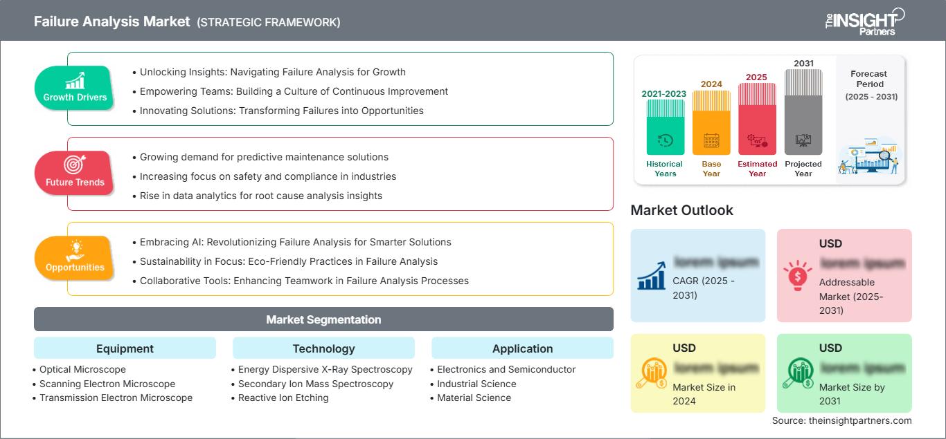
Failure Analysis Market: Strategic Insights
Regional Insights
North America Failure Analysis Market
North America held 30–34% of global revenue in 2025 and is expected to expand at a 7.6–8.2% CAGR through 2034. Its Failure Analysis Market share is a function of heavy semiconductor designs, reliability programs in the aerospace and defense industry, medical device quality systems, and established university and independent laboratories. Government initiatives for manufacturing, advanced packaging, and research infrastructure are driving the need for microscopy, spectroscopy, and sample preparation capabilities near manufacturing plants.
The buying trend in the Failure Analysis Market is moving towards fully integrated systems that minimize expert involvement and enhance traceability in high-value applications. The USA drives the regional spending, while Canada brings in high-end material research, mining, energy, and academia. Service response, application engineering, and workflow validation impact the choice of vendors as the prolonged downtime of the instrument can hamper yield optimization or product release. Growth will continue to be even in new instruments, software upgrade, detectors, and outsource testing.
U.S. Failure Analysis Market
The US represented 78–82% of North American revenue in 2025 and is projected to grow at a 7.8–8.4% CAGR during 2026–2034. With semiconductor developments in Arizona, Texas, New York, Ohio, and other industrial areas, the country has been expanding its laboratory customer base. In addition, there exist considerable aerospace and defense, automotive, energy, and biomedical research markets in the country, diversifying the demand for investigations that do not only focus on integrated circuits and packaging.
Thermo Fisher Scientific Inc., Carl Zeiss AG, JEOL USA, Inc., Bruker Corporation, Intertek Group plc, and other vendors have business dealings with US laboratories. The applications of the technology have been shifting towards advanced packaging, wide bandgap power electronics, batteries, additive manufacturing, and contamination control. Buyers are now demanding a combination of non-destructive imaging with scanning electron microscopy (SEM), focused ion beam (FIB), energy-dispersive x-ray (EDX), or secondary ion mass spectrometry (SIMS).
Europe Failure Analysis Market
Europe accounted for 22–26% share in 2025 and should register a 7.2–7.8% CAGR through 2034, with Germany leading regional demand. German advantages include automotive electronics, industrial machinery, material sciences, and semiconductor investment, creating the need for fracture, contamination, and electronic reliability analysis. UK provides compound semiconductor research, aerospace industry, universities, and outsourcing laboratories, which help in conducting studies for industry and emerging technologies.
The French combine aerospace, microelectronics, nuclear and research facilities to perform valuable instrument applications. Italy includes power electronics, automotive industry, and material laboratories, whereas Spain expands into renewable energy materials, automotive industry, and university labs. There is a European policy for increased semiconductor manufacturing, creating an encouragement for pilot lines and production facilities that require process diagnostics. Providers with services in the region, multi-lingual applications, and process workflows in accordance with traceability and quality regulations have an edge.
APAC Failure Analysis Market
Asia Pacific held 34–38% of the Failure Analysis Market in 2025 and is forecast to grow at an 8.8–9.4% CAGR through 2034, making it the fastest-growing region. China leads by scale, while Japan and South Korea combine advanced semiconductor, display, battery, and materials capabilities. India is expanding electronics manufacturing and laboratory infrastructure, and Australia contributes mining, energy materials, and university research.
Industrial policy, fab construction, advanced packaging, and local supply-chain development support equipment demand. Dense production clusters favor rapid fault isolation, automated defect review, and high-throughput sample preparation. Regional buyers also prioritize local service coverage and training to sustain utilization across large installed bases.
Middle East & Africa Failure Analysis Market
The Middle East and Africa market is expected to expand at a 6.6–7.2% CAGR through 2034. Saudi Arabia leads through energy, petrochemicals, mining, infrastructure, and research investment. The UAE supports aviation, advanced manufacturing, and university laboratories, while South Africa contributes mining, metallurgy, power, and established materials-engineering capabilities.
Rest of MEA demand remains project-led, frequently relying on centralized laboratories or outsourced expertise. Growth opportunities involve corrosion, weld integrity, pipeline and turbine components, construction materials, and localized electronics research. Supplier success depends on training, remote diagnostics, dependable consumables, and partnerships that overcome limited specialist availability.
Segmentation Analysis
Equipment
Equipment is projected to expand at a 7.9–8.5% CAGR during 2026–2034. The Failure Analysis Market scope covers complementary platforms selected by feature size, material, depth, preparation requirements, and acceptable destructiveness. Laboratories increasingly build correlative workflows rather than rely on a single instrument, supporting upgrades in detectors, automation, navigation, and sample transfer. Capital intensity favors shared facilities and outsourced services where utilization is intermittent.
- Optical Microscope: Optical systems remain the first-line screening tool for surface damage, contamination, fractures, and assembly defects, offering rapid navigation before higher-resolution or destructive investigation.
- Scanning Electron Microscope: SEM leads routine high-resolution imaging because it combines surface morphology, compositional contrast, broad sample compatibility, and EDX integration across electronics and materials laboratories.
- Transmission Electron Microscope: TEM serves atomic-scale crystallography, interfaces, precipitates, and nanoscale defects, making it strategically important for advanced-node semiconductors, batteries, catalysts, and novel materials.
- Focused Ion Beam: FIB enables site-specific cross-sectioning, circuit editing, and TEM lamella preparation, with demand rising as buried defects and multilayer structures become harder to access.
- Scanning Probe Microscope: SPM provides nanoscale topography and local mechanical, electrical, or surface-property measurements, supporting semiconductor, coating, polymer, and functional-material investigations.
- Dual Beam: Integrated FIB-SEM platforms combine milling and imaging in one chamber, reducing transfer errors and accelerating targeted analysis of complex packages, devices, and material interfaces.
Technology
Technology is forecast to grow at an 8.1–8.7% CAGR through 2034. Technique selection depends on whether investigators need elemental composition, isotopic or depth sensitivity, or controlled material removal. Demand increasingly favors multimodal evidence, with EDX supporting rapid screening, SIMS resolving trace chemistry and depth profiles, and reactive ion etching enabling selective preparation. Software linking images, spectra, and process history improves interpretation and reproducibility.
- Energy Dispersive X-Ray Spectroscopy: EDX is widely paired with electron microscopy for rapid elemental identification and mapping, supporting contamination analysis, inclusions, coatings, solder joints, and fracture-surface investigations.
- Secondary Ion Mass Spectroscopy: SIMS addresses trace elements, dopants, isotopes, and depth profiling, making it important for semiconductor process control, thin films, batteries, and surface chemistry.
- Reactive Ion Etching: RIE provides controlled, material-selective removal that helps expose buried structures and prepare layered devices while limiting mechanical deformation associated with conventional polishing.
Application
Application is expected to expand at an 8.0–8.6% CAGR during 2026–2034. Electronics and semiconductor demand sets requirements for resolution and throughput, while industrial and material sciences broaden utilization across metals, coatings, composites, and energy systems. Bioscience adds specialized imaging and preparation needs. Procurement increasingly reflects workflow-specific risk, including defect accessibility, evidence preservation, regulatory requirements, and the cost of delayed corrective action.
- Electronics and Semiconductor: This application dominates demand as shrinking features, advanced packaging, power devices, and higher reliability targets require rapid localization, cross-sectioning, compositional analysis, and yield-learning feedback.
- Industrial Science: Manufacturers use failure analysis to investigate fatigue, corrosion, wear, welds, additive components, and supplier defects, linking laboratory evidence to maintenance and process improvement.
- Material Science: Research teams characterize microstructure, interfaces, phases, coatings, and degradation in batteries, catalysts, alloys, ceramics, polymers, and composites supporting next-generation industrial products.
- Bioscience: Bioscience laboratories apply advanced microscopy and preparation to cellular ultrastructure, biomaterials, medical devices, and tissue interfaces, emphasizing contrast, preservation, and reproducible protocols.
Opportunity Snapshot
| Application | Revenue Contribution | Trend Tag | Adoption Stage |
| Electronics and Semiconductor | High | Advanced Packaging | Scaling |
| Industrial Science | High | Predictive Reliability | Mature |
| Material Science | Medium | Battery Interfaces | Scaling |
| Bioscience | Low | Correlative Imaging | Emerging |
Failure Analysis Market Growth Drivers and Impact Analysis
Advanced packaging raises defect-localization complexity
Defects associated with chiplets, hybrid bonding, high bandwidth memory, through silicon via, and hetero-materials occur under several layers of interfaces. Surface inspection cannot reliably detect voids, cracks, delamination, contamination, and electrical discontinuity without risk of destroying the evidence. Therefore, labs use a combination of X-ray localization, laser or ion beam extraction, scanning electron microscopy (SEM), energy dispersive X-ray spectroscopy (EDX), and transmission electron microscopy (TEM). It leads to higher equipment investment per procedure and need for better coordinate alignment, automation, and preparation repeatability. However, the commercial significance is not limited to the advanced fabs since the needs of outsourced labs, packagers, automotive electronics suppliers, and power device manufacturers are no different.
Manufacturing investment expands the analytical installed base
Not only do new semiconductor and advanced packaging developments generate demand for production equipment but process development, qualification, contamination control, and reliability labs as well. Each of them requires analytical capability in design, ramp, and production stages, and supplier networks need independent validation and support. Governmental motivation in the US, Europe, and Asia boosts the effect even more by making regional material, equipment, and packaging capabilities attractive. Market effects from this include instrument purchases, lab builds, service agreements, training programs, and outsourcing. Since analytical equipment helps at multiple process stages and product generations, investment continues after fab build. Supplier companies that have locally-based applications and parts logistics are well positioned to win both initial deployments and future upgrades.
Reliability economics favor earlier root-cause detection
Costs of failure skyrocket once the defects leave the wafer and component production processes and reach module, system, field service, or safety-critical environments. In order to deal with this challenge, the producers push the analytical process further up in development and control by means of microscopy and spectroscopy to ensure material, interface, and correction validation prior to scale up. This requirement is heightened in the cases of automotive electrification, aerospace qualification, medical device, and industrial automation because of possible recall issues, production stoppage, or requalification period. The effect on procurement becomes a switch from rare forensic testing to regular reliability routines, standardized procedures, and reporting.
Failure Analysis Market Future Trends
AI-guided multimodal investigation
Failure Analysis Market trends will focus more and more on artificial intelligence that correlates images, spectra, process metadata, and previous examples across several pieces of instrumentation. Algorithms will help with feature detection, segmentation, ranking of anomalies, and navigation while allowing the expert to decide on causality. The next stage is not the autonomous microscopy but the orchestration of the closed workflow: non-destructive scanning spots the candidate sites, software translates the coordinates, milling recipes uncover the targets, and analysis updates the course of the investigation. The companies will compete with each other on their governance, explainability, cybersecurity, and the ability to work with customer data environments.
Low-damage, high-throughput sample preparation
Sample preparation will turn into a key competitive arena as structures get thicker, have multiple layers, and become sensitive to heat and ions. The use of hybrid sample preparation techniques involving combinations of laser ablation, plasma FIB, broad ion beam milling, cooling, and low kV polishing will result in a reduction in the time to access the sample while keeping the interfaces intact. The use of automated endpoints and recipes for the sample preparation procedure will lead to less variability on the part of operators and will make the complicated process available to everyone. Instrument manufacturers will start designing sample preparation and imaging together with the same coordinate system and contamination control.
Failure Analysis Market Opportunities
Regional application centers and shared laboratories
Both suppliers and investors have an opportunity to create application labs close to emerging semiconductor, battery, and advanced materials hubs where clients require demonstrations, methods development, training, and overflow analysis before making capital investments. A shared lab concept is useful in reducing barriers to market entry for small-scale manufacturers and turning sporadic demand into increased utilization rates. Sources of income will range from access to instruments, fee-based projects, subscriptions, training, and services agreements. Ideal markets would be US fab corridors, European pilot line networks, Indian electronics hubs, and Southeast Asian packaging nodes. Collaborations with universities and independent labs are helpful in establishing credibility and developing talent.
Workflow modernization for installed instruments
A large installed base creates an opportunity to sell productivity improvements without requiring full system replacement. Vendors can package detector upgrades, automation modules, AI-assisted analysis, remote diagnostics, cybersecurity, and standardized application recipes around existing SEM, FIB, TEM, and spectroscopy tools. Customers gain shorter investigations and improved reproducibility while preserving validated capital assets. Commercial models may include outcome-based service tiers, software subscriptions, and phased upgrades aligned with utilization. Integrators should focus on open data exchange and coordinate transfer across brands because many laboratories operate mixed fleets. The strongest propositions will quantify fewer repeat preparations, higher uptime, reduced training time, and faster corrective-action closure.
Recent Developments
- July 2026: Keysight Technologies has introduced Keysight Multiphysics, a new design and verification solution aimed at helping engineers identify potential failures in complex electronic products earlier in the development process. Modern electronic systems increasingly combine electrical, thermal, mechanical, and optical technologies in compact designs. Because these physical domains interact with one another, a problem in one area can create unexpected issues in another. Traditional engineering approaches often examine these effects separately, meaning some reliability problems may only become visible after a physical prototype has been built.
- November 2025: ZEISS Microscopy is showcasing its latest technologies for semiconductor failure analysis at the 51st International Symposium for Testing & Failure Analysis (ISTFA), held November 16–20, 2025, at the Pasadena Convention Center in California. At the event, ZEISS is presenting seven technical papers and two tutorials covering advanced imaging and analytical techniques for semiconductor failure analysis. Key topics include AI-based image segmentation, automation, power-device analysis, hybrid-bond inspection, and correlative microscopy.
- September 2025: Chemnitz, Germany: scia Systems announced new capabilities for semiconductor manufacturing and failure analysis ahead of SEMICON West 2025, highlighting advances in ion beam etching and thin-film processing. The company is focusing particularly on applications involving advanced packaging, AI processors, MEMS, sensors, optics, and photonics.
Frequently Asked Questions

- Comprehensive Market Sizing and Forecast Analysis
- Detailed Segmentation Analysis
- In-Depth Market Dynamics Assessment
- Regional and Country-Level Insights
- Competitive Landscape and Company Benchmarking
- Strategic Business Intelligence
Recent Reports
Testimonials

The Insight Partners provided valuable market intelligence that supported our global go-to-market strategy. Their team was professional, responsive, and attentive to our feedback, providing thoughtful analysis and helpful methodological clarifications throughout the project.
Junmo Kim Chief Financial Officer (CFO), Enertech Co., Ltd.
The Insight Partners' SCADA System Market report is comprehensive, with valuable insights on current trends and future forecasts. The team was highly professional, responsive, and supportive throughout. We are very satisfied and highly recommend their services.
RAN KEDEM Partner, Reali Technologies LTDs
I requested a report on a very specific software market and the team produced the report in a few days. The information was very relevant and well presented. I then requested some changes and additions to the report. The team was again very responsive and I got the final report in less than a week.
JEAN-HERVE JENN Chairman, Future Analytica
We worked with The Insight Partners for an important market study and forecast. They gave us clear insights into opportunities and risks, which helped shape our plans. Their research was easy to use and based on solid data. It helped us make smart, confident decisions. We highly recommend them.
PIYUSH NAGPAL Sr. Vice President, High Beam Global
The Insight Partners delivered insightful, well-structured market research with strong domain expertise. Their team was professional and responsive throughout. The user-friendly website made accessing industry reports seamless. We highly recommend them for reliable, high-quality research services
YUKIHIKO ADACHI CEO, Deep Blue, LLC.
This is the first time I have purchased a market report from The Insight Partners.While I was unsure at first, I visited their web site and felt more comfortable to take the risk and purchase a market report.I am completely satisfied with the quality of the report and customer service. I had several questions and comments with the initial report, but after a couple of dialogs over email with their analyst I believe I have a report that I can use as input to our strategic planning process.Thank you so much for taking the extra time and making this a positive experience.I will definitely recommend your service to others and you will be my first call when we need further market data.
JOHN SUZUKI President and Chief Executive Officer, Board Director, BK Technologies
I wish to appreciate your support and the professionalism you displayed in the course of attending to my request for information regarding to infectious disease IVD market in Nigeria. I appreciate your patience, your guidance, and the fact that you were willing to offer a discount, which eventually made it possible for us to close a deal. I look forward to engaging The Insight Partners in the future, all thanks to the impression you have created in me as a result of this first encounter.
DR CHIJIOKE ONYIA MANAGING DIRECTOR, PineCrest Healthcare Ltd.Reason to Buy
- Informed Decision-Making
- Understanding Market Dynamics
- Competitive Analysis
- Identifying Emerging Markets
- Customer Insights
- Market Forecasts
- Risk Mitigation
- Boosting Operational Efficiency
- Strategic Planning
- Investment Justification
- Tracking Industry Innovations
- Aligning with Regulatory Trends





 Get Free Sample for