
UV Tapes Market Demand, Size & Forecast by 2034
Coverage: by Product Type (Polyolefin (PO) UV Tape, Polyvinyl Chloride (PVC) UV Tape, Polyethylene Terephthalate (PET) UV Tape, Others); Application (Wafer Dicing, Back Grinding, Others) , and Geography (North America, Europe, Asia Pacific, and South and Central America)
- Status : Data Released
- Report Code : TIPRE00008291
- Category : Electronics and Semiconductor
- No. of Pages : 150
- Available Report Formats :


- Last update date : September 17, 2026


2025 Market Size
US$ 666.4 Mn
Base year value
2034 Forecast
US$ 1,582.62 Mn
Projected by 2034
CAGR 2026-2034
10.09 %
Growth rate
Addressable Market
US$ 10,000.24 Mn
(2026-2034)
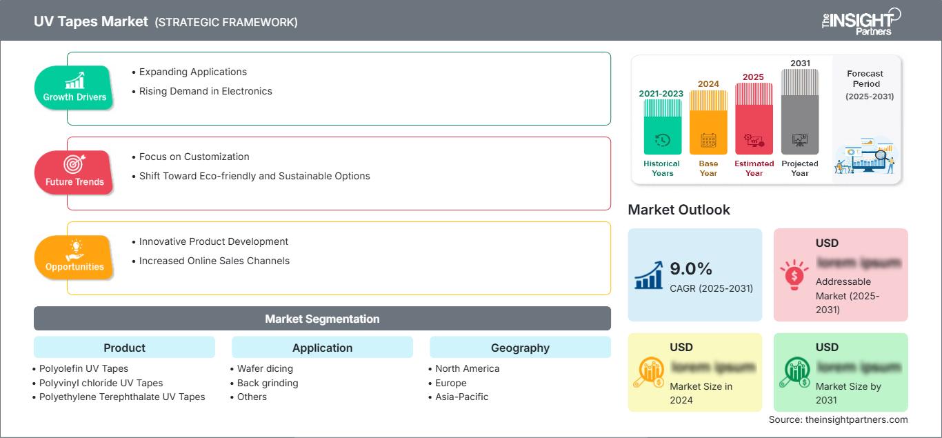
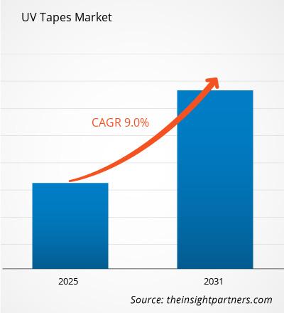
The UV tapes market is valued at US$ 666.4 Million in 2025 and is expected to reach US$ 1,582.62 Million by 2034, registering a CAGR of 10.09% during 2026–2034. The market covers UV-responsive adhesive tapes used across semiconductor wafer processing, particularly dicing and back grinding, where controlled adhesion, clean release, dimensional stability, and compatibility with increasingly thin and complex wafers are essential.
North America is positioned for steady expansion, supported by semiconductor fabrication investments, advanced packaging activity, and rising demand for process materials that improve wafer handling precision. The uv tapes market size is also benefiting from reshoring initiatives, domestic chip manufacturing programs, and greater adoption of compound semiconductor devices requiring specialized temporary bonding and dicing solutions.
UV Tapes Market Assessment and Insights
- North America accounts for a 23–27% share in 2025 and is expected to grow at a 9.2–10.2% CAGR between 2026 – 2034, supported by semiconductor capacity expansion, advanced packaging, and demand for high-precision wafer-processing materials.
- US represents 72–76% of North America's 2025 market and is projected to grow at a 9.5–10.5% CAGR between 2026 – 2034, led by domestic semiconductor manufacturing and advanced packaging investments.
- Europe holds an estimated 18–22% share in 2025 and is expected to expand at a 8.8–9.8% CAGR between 2026 – 2034, with Germany, the UK, France, Italy, and Spain supporting automotive, industrial, and specialty semiconductor applications.
- Asia Pacific represents approximately 45–49% share in 2025 and is projected to register a 10.8–11.8% CAGR between 2026 – 2034, led by China, Japan, South Korea, Taiwan-linked supply chains, India, and Southeast Asian manufacturing clusters.
- Largest Segment: Wafer dicing holds a 62–66% market share in 2025 and is expected to grow at a 10.4–11.4% CAGR between 2026 – 2034, reflecting its central role in singulation.
- High Growth Segment: Polyethylene Terephthalate UV Tapes account for a 10–14% market share in 2025 and are projected to grow at a 12.0–13.0% CAGR between 2026 – 2034, supported by dimensional stability and specialized wafer-processing requirements.
- Key companies analyzed in detail: Denka Company Limited; Furukawa Electric Co., Ltd.; LINTEC OF AMERICA, INC.; Loadpoint Ltd.; Mitsui Chemicals America, Inc.; Nippon Pulse Motor Taiwan; Nitto Denko Corporation; Pantech Tape Co., Ltd.; Sumitomo Bakelite Co., Ltd.; Ultron Systems, Inc.
Source: The Insight Partners' analysis based on proprietary research, government publications, company annual reports, investor presentations, industry databases, and expert interviews.
The market has moved from the use of traditional wafer-retention materials to the development of specialized tapes that can ensure sufficient holding power before UV and controlled release after the treatment. Wafer thinning, compound semiconductors, laser wafer singulation, and higher contamination requirements mean moving towards thin backings, specially tailored acrylics, anti-static properties, and reliable releasing behavior. The production of such materials is becoming more application-driven rather than focusing on one tape type.
Going forward, investments will be made in Asia semiconductor ecosystems as well as adding capacities in North America and Europe to increase local demand resilience. Regulatory push towards semiconductor localization, diversification, and efficient manufacturing will favor process material investments. Suppliers with coating technology flexibility, technical expertise in their local markets, and qualifications will have an advantage in addressing the needs of integrated device manufacturers, outsourced semiconductor assembly and test companies, and specialty chipmakers.
UV Tapes Market Report Scope
| Report Attribute | Details |
|---|---|
| Market size in 2025 | US$ 666.4 Million |
| Market Size by 2034 | US$ 1,582.62 Million |
| Global CAGR (2026 - 2034) | 10.09% |
| Historical Data | 2021-2024 |
| Forecast period | 2026-2034 |
UV Tapes Market Analysis
Demand is closely linked to wafer starts, chip miniaturization, and the number of processing steps requiring temporary fixation. The value chain spans polymer-film producers, adhesive formulators, coating and converting specialists, equipment suppliers, semiconductor manufacturers, and packaging houses. The uv tapes market growth therefore, depends not only on semiconductor volumes but also on yield improvement requirements, wafer thickness reduction, and adoption of compound materials such as SiC and GaN.
The supply dynamics depend on coating know-how, adhesive technology, clean manufacturing, and qualification cycle times, which can make switching customers difficult. Consistency of product is especially critical since differences in adhesive thickness or release properties could affect chipping, die pick-up, residues, and even wafer breakage. Suppliers differentiate themselves with application engineering, custom backing materials, antistatics, and compatibility with blade, stealth, and laser dicing processes.
Competitiveness is primarily among Japanese, European, and US-based specialty material suppliers who already have semiconductor customers. Denka Company Limited and Nitto Denko Corporation offer general process materials, while Furukawa Electric Co., Ltd. focuses on semiconductor tapes and dicing-related materials. LINTEC OF AMERICA, INC. benefits from the broader Adwill platform, while Sumitomo Bakelite Co., Ltd. combines dicing-tape expertise with semiconductor packaging materials, according to the UV Tapes Market report.
Strategic positioning increasingly depends on co-development and process integration rather than tape supply alone. Mitsui Chemicals America, Inc. has exposure to high-clean wafer-processing tapes, while Pantech Tape Co., Ltd., Ultron Systems, Inc., Loadpoint Ltd., and Nippon Pulse Motor Taiwan serve specialized process requirements. Investment priorities include cleaner adhesive systems, thin-wafer handling, automation compatibility, and regional technical support, allowing suppliers to protect margins through differentiated performance rather than volume competition.
● REPORT CUSTOMIZATION
Tailor This Report To Align With Your Specific Business Requirements
This report can be customized to align precisely with your business objectives, scope, and target markets. Customization options include tailored segmentation, geography, competitive analysis, and strategic insights to support informed decision-making.
Customize This Report →WHAT YOU CAN ADJUST
- ● Segmentations
- ● Geography
- ● Competitive Analysis
- ● Language Preferences
UV Tapes Market: Strategic Insights
Regional Insights
North America uv tapes market
North America is estimated to represent 23–27% of the global uv tapes market demand in 2025 and is expected to expand at a 9.2–10.2% CAGR through 2034. US dominance is seen in the region owing to the activities in semiconductor fabrication, advanced packaging, aerospace electronics, automotive semiconductors, and specialty devices. The domestic production drive is driving up the requirement for process materials, while regional technical support is increasingly becoming significant in view of shorter supply chains.
The regional environment creates favorable conditions for the utilization of high-performance tapes that can adhere well during the processing of wafers through grinding and dicing and then releasing the same after exposure to UV light. Compound semiconductors and thin wafers are also driving up demand. The contribution of Canada is selective through its activities in the field of electronics and research. The US, however, is the major demand center in the region.
U.S. uv tapes Market
The US represents approximately 72–76% of North America's 2025 uv tapes market demand and is projected to grow at a 9.5–10.5% CAGR through 2034. Semiconductor localization, advanced packaging investments, and increased manufacturing of automotive, AI, communication, and power semiconductors are key structural drivers of demand. The portfolio of applications consists mainly of dicing and back-grinding services, with high-value specialty semiconductors demanding higher precision manufacturing processes.
Presence within the company involves participation in the worldwide suppliers of materials and specialists in tape manufacturing for semiconductor fabs, packagers, and equipment. Newer demands involve tapes for thin wafers, compound semiconductor substrate support, antistatic performance, and reduced residue release. The long qualification process may be a competitive advantage due to the involvement of technical cooperation and specific process validation. Therefore, the US market will benefit from the suppliers who combine consistency and application engineering skills.
Europe uv tapes Market
Europe is estimated to hold an 18–22% of the uv tapes market share in 2025 and is expected to grow at an 8.8–9.8% CAGR through 2034. Germany is the leading country, supported by automotive semiconductor demand, industrial automation, power electronics, and established semiconductor equipment capabilities.
The UK makes its contribution by means of the development of compound semiconductors, photonics and electronics, requiring materials for the processing of special wafers. The German market is represented by the automotive and industrial semiconductor market and is characterized by steady demand for reliable processing tapes. In France, there are possibilities for development in aerospace, defense electronics and power devices. Italy and Spain make their contributions via automotive, industrial electronics and semiconductor-related investments. European customers usually appreciate process reliability, ecological requirements, material supplies and technical documents.
APAC uv tapes Market
APAC represents approximately 45–49% of the global uv tapes market demand in 2025 and is projected to grow at a 10.8–11.8% CAGR through 2034. China, Japan, and South Korea form the core demand base, while India and Australia offer emerging opportunities through semiconductor localization and electronics manufacturing policies.
China remains the leading market, supported by domestic semiconductor investment, while Japan retains strong materials expertise. South Korea benefits from memory and advanced semiconductor production. India is developing a broader semiconductor manufacturing ecosystem, and Australia remains smaller but relevant to research and specialty applications. Regional demand is reinforced by electronics exports, packaging capacity, compound semiconductor adoption, and government-supported manufacturing programs.
Middle East & Africa uv tapes Market
The Middle East and Africa uv tapes market represents a smaller demand base but is projected to expand at a 6.5–7.5% CAGR through 2034. Saudi Arabia and the UAE are the leading regional opportunities as economic diversification initiatives encourage electronics, industrial technology, and advanced manufacturing investment.
South Africa provides a specialized electronics and research base, while the rest of MEA remains dependent on imported semiconductor materials and equipment. Infrastructure development, data-center investment, telecommunications modernization, and diversification beyond hydrocarbons can gradually expand semiconductor-related applications. Demand will remain concentrated in imported wafers, packaging, and specialty electronics rather than large-scale local wafer fabrication, making distributor networks and technical service capabilities important routes to market.
Segmentation Analysis
Product
Product selection is governed by backing-film strength, elongation, UV response, adhesive cleanliness, and compatibility with wafer geometry. Polyolefin remains important for balanced flexibility and process handling, while PET supports dimensional stability. PVC retains specialized applications where established processing characteristics remain advantageous. The product segment is expected to grow at a 10.0–10.8% CAGR during 2026–2034 as manufacturers optimize tape construction for thinner and more complex wafers across the UV Tapes Market.
- Polyolefin UV Tapes provide flexibility, controlled elongation, and dependable handling during wafer processing, making them important for applications requiring balanced adhesion, expansion behavior, and compatibility with automated mounting systems.
- Polyvinyl chloride UV Tapes remain relevant where established converting characteristics, mechanical performance, and process familiarity support existing semiconductor production flows and qualification requirements.
- Polyethylene Terephthalate UV Tapes provide dimensional stability and controlled film behavior, supporting demanding wafer-processing applications where precise positioning and reduced deformation are strategically important.
- Others include specialized film constructions developed for application-specific requirements, including antistatic performance, high transparency, or compatibility with emerging semiconductor materials.
Application
Application demand is centered on processes where wafer stability and predictable release directly influence yield. Wafer dicing remains the principal use because tapes must hold wafers during singulation and enable efficient die pickup after UV exposure. Back grinding requires protection and dimensional control as wafer thickness decreases. The application segment is projected to grow at a 10.2–11.0% CAGR through 2034.
- Wafer dicing remains the dominant application because controlled adhesion supports accurate singulation, reduces chip movement, and facilitates efficient die pickup after UV irradiation.
- Back grinding requires tapes that protect patterned surfaces while maintaining stable adhesion during mechanical thinning, particularly as semiconductor manufacturers process increasingly thin wafers.
- Others cover specialized temporary retention and handling processes where UV-controlled adhesion provides controlled transfer, protection, or release within semiconductor manufacturing flows.
Geography
Geographic demand reflects semiconductor manufacturing concentration, advanced packaging capacity, and regional investment incentives. APAC remains the largest demand center, while North America benefits from localization initiatives and Europe from automotive and industrial semiconductor applications. The geography segment is expected to expand at a 9.6–10.4% CAGR during 2026–2034 as semiconductor supply chains diversify across established and emerging manufacturing hubs in the UV Tapes Market.
- North America offers high-value demand driven by semiconductor fabrication, advanced packaging, specialty electronics, and domestic supply-chain development.
- Europe maintains a technology-intensive customer base supported by automotive electronics, industrial semiconductors, power devices, and specialized manufacturing.
- Asia-Pacific provides the largest production ecosystem, encompassing major semiconductor, packaging, electronics, and materials clusters across China, Japan, South Korea, India, and Southeast Asia.
- South and Central America represent an emerging opportunity where electronics assembly, industrial automation, and imported semiconductor components create selective requirements for wafer-processing materials.
- Middle East and Africa remain smaller markets, with opportunities linked to electronics modernization, infrastructure investment, research activity, and economic diversification programs.
Opportunity Snapshot
| Application | Revenue Contribution (High/Medium/Low) | Trend Tag (MAX 2 words) | Adoption Stage (Emerging/Scaling/Mature) |
| Wafer dicing | High | Precision Singulation | Mature |
| Back grinding | High | Thin Wafer | Scaling |
| Others | Low | Process Transfer | Emerging |
UV Tapes Market Growth Drivers and Impact Analysis
Rising Demand for Thin and Advanced Semiconductor Wafers
As wafer and die sizes continue to decrease, there will be an increased need for temporary bonding materials that can endure mechanical treatment without destroying fragile components. Thinner wafers are more prone to breakage, bowing, chipping, and handling loss, making it critical for the adhesive to have uniformity and to release controllably. This trend will positively impact materials with unique UV response properties since the adhesive strength could be retained through the grinding/dicing step but then reduced post-UV treatment. The need for such tapes is particularly high for memory, power electronics, compound semiconductors, and advanced packaging. Manufacturers who can deliver low levels of contamination while offering support on thinner substrates would benefit from obtaining qualifications with higher value. The commercial benefit is not just driven by tape volume but also by proprietary process formulations.
Expansion of Semiconductor Manufacturing and Packaging Capacity
New investments in wafer processing capabilities – fab construction, assembly, testing and packaging – broaden the addressable market for the wafer-processing consumables. Construction and subsequent production ramp-ups in Asian, North American, and select European locations drive the need for consumables in dicing, back grinding, temporary bonding, and other process applications. As the new fabs shift from tool installations to qualification and volume production, tape suppliers have the chance to sell their products into the process development phase of the factory operations, as opposed to relying solely on replacement orders. Diversification of capacity investments provides additional incentive for semiconductor producers to qualify several suppliers for their products, thus creating additional opportunities for suppliers of technologically differentiated products. The effect is especially pronounced for tape suppliers providing regional technical expertise, timely product sampling, and reliable manufacturing quality.
Greater Adoption of Compound and Power Semiconductor Materials
Newer substrate technologies, such as silicon carbide and gallium nitride, present mechanical and surface properties different from those presented by traditional silicon substrates, necessitating the need for new tapes that will be designed to suit the unique cutting, grinding, and release needs presented by these newer substrates. Processing of compound semiconductors may require higher hardness, special chipping tendencies, and special wafer dimensions that require special adhesive structures. As electric vehicles, energy-generating systems, data centers, and high-frequency communications increase the demand for power and compound semiconductors, there will be an increase in the commercial relevance of the wafer processing demands. UV tapes are able to retain stable adhesion while being processed and releasing them at will helps in improving yields in this type of application. Formulations available for substrates such as SiC, GaN, glass, and other hard-to-process substrates can offer a competitive advantage through their performance.
UV Tapes Market Future Trends
Integration of UV Tapes with Automated Wafer Handling
Automation will increasingly influence tape selection as semiconductor factories pursue higher throughput and lower process variability. Future tape designs are likely to emphasize predictable peel behavior, stable dimensions, antistatic characteristics, and compatibility with automated mounting and peeling systems. Integration with inspection and process-control equipment can further reduce operator intervention and improve traceability. Suppliers may increasingly provide tape-and-equipment combinations rather than standalone consumables, particularly where precise application tension and UV exposure affect release performance. The UV tapes market trends will therefore shift toward products engineered around complete process windows instead of isolated adhesive specifications. Digital monitoring of tape application, UV dosage, and peel performance could become more common in advanced facilities. This trend should reward manufacturers capable of combining material science, converting expertise, automation compatibility, and application engineering within a single customer qualification framework.
Development of Cleaner and More Application-Specific Adhesive Systems
Requirements for environmental cleanliness and yield sensitivity will lead to innovations in the production of less residual adhesives with better stability and controlled release. The semiconductor industry is now becoming more and more concerned about contamination control as a factor of process quality, especially with regard to advanced processes, thin wafers, and highly integrated packages. Consequently, future products will probably incorporate adhesives with optimized chemistry and backings for tight process tolerances. Transparency for laser processability, antistatic properties, and good adhesion to compound semiconductor substrates might be some of the criteria used to differentiate products in the future. In the future, the trend will involve more customization of adhesives as opposed to product lines with little flexibility. With the toughening of qualifications, the capability to demonstrate consistent material and process behavior will be an influencing factor in procurement decisions.
UV Tapes Market Opportunities
Localization of Technical Support and Supply Chains
The geographic diversification of semiconductor manufacturing creates an opportunity for UV tape suppliers to establish regional technical centers, convert capacity, and inventory hubs close to emerging fabrication clusters. Localized support can shorten qualification cycles, accelerate troubleshooting, and reduce supply risks associated with long international logistics routes. India, Southeast Asia, and North America offer particularly relevant opportunities as semiconductor ecosystems broaden. Companies can pursue partnerships with equipment providers, packaging houses, and local distributors to build application-specific support rather than relying exclusively on centralized sales organizations. The uv tapes market scope is consequently expanding beyond material supply toward integrated process support. Investments in regional laboratories can also allow suppliers to test tape behavior against locally used wafer materials and equipment. Such localization can improve customer retention, reduce response times, and create barriers against competitors lacking established technical infrastructure.
Specialized Solutions for Compound Semiconductor Processing
Compound semiconductor manufacturing presents an opportunity for suppliers to develop premium tape solutions tailored to SiC, GaN, sapphire, glass, and other difficult substrates. These materials can require different adhesive strengths, cutting behaviors, flexibility, and release profiles compared with conventional silicon. Suppliers can target power electronics, electric vehicles, charging systems, optical devices, and high-frequency communications applications through dedicated product qualification programs. The opportunity is particularly attractive where wafer value is high and yield losses have significant financial consequences. Companies can combine application testing with customer co-development to optimize adhesive chemistry, backing thickness, UV response, and antistatic properties. As device manufacturers scale production, successful qualification can translate into recurring consumable demand. The uv tapes market forecasts indicate that specialized applications can become an important source of value creation as advanced substrate adoption broadens.
Frequently Asked Questions

- Comprehensive Market Sizing and Forecast Analysis
- Detailed Segmentation Analysis
- In-Depth Market Dynamics Assessment
- Regional and Country-Level Insights
- Competitive Landscape and Company Benchmarking
- Strategic Business Intelligence
Recent Reports
Testimonials

The Insight Partners' SCADA System Market report is comprehensive, with valuable insights on current trends and future forecasts. The team was highly professional, responsive, and supportive throughout. We are very satisfied and highly recommend their services.
RAN KEDEM Partner, Reali Technologies LTDs
I requested a report on a very specific software market and the team produced the report in a few days. The information was very relevant and well presented. I then requested some changes and additions to the report. The team was again very responsive and I got the final report in less than a week.
JEAN-HERVE JENN Chairman, Future Analytica
We worked with The Insight Partners for an important market study and forecast. They gave us clear insights into opportunities and risks, which helped shape our plans. Their research was easy to use and based on solid data. It helped us make smart, confident decisions. We highly recommend them.
PIYUSH NAGPAL Sr. Vice President, High Beam Global
The Insight Partners delivered insightful, well-structured market research with strong domain expertise. Their team was professional and responsive throughout. The user-friendly website made accessing industry reports seamless. We highly recommend them for reliable, high-quality research services
YUKIHIKO ADACHI CEO, Deep Blue, LLC.
This is the first time I have purchased a market report from The Insight Partners.While I was unsure at first, I visited their web site and felt more comfortable to take the risk and purchase a market report.I am completely satisfied with the quality of the report and customer service. I had several questions and comments with the initial report, but after a couple of dialogs over email with their analyst I believe I have a report that I can use as input to our strategic planning process.Thank you so much for taking the extra time and making this a positive experience.I will definitely recommend your service to others and you will be my first call when we need further market data.
JOHN SUZUKI President and Chief Executive Officer, Board Director, BK Technologies
I wish to appreciate your support and the professionalism you displayed in the course of attending to my request for information regarding to infectious disease IVD market in Nigeria. I appreciate your patience, your guidance, and the fact that you were willing to offer a discount, which eventually made it possible for us to close a deal. I look forward to engaging The Insight Partners in the future, all thanks to the impression you have created in me as a result of this first encounter.
DR CHIJIOKE ONYIA MANAGING DIRECTOR, PineCrest Healthcare Ltd.Reason to Buy
- Informed Decision-Making
- Understanding Market Dynamics
- Competitive Analysis
- Identifying Emerging Markets
- Customer Insights
- Market Forecasts
- Risk Mitigation
- Boosting Operational Efficiency
- Strategic Planning
- Investment Justification
- Tracking Industry Innovations
- Aligning with Regulatory Trends





 Get Free Sample for